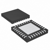
MAX1531ETJ+T Maxim Integrated Products, MAX1531ETJ+T Datasheet - Page 30

MAX1531ETJ+T
Manufacturer Part Number
MAX1531ETJ+T
Description
IC PS CTRLR MULTI-OUTPUT 32TQFN
Manufacturer
Maxim Integrated Products
Datasheet
1.MAX1531ETJT.pdf
(33 pages)
Specifications of MAX1531ETJ+T
Applications
Five Power Supply Monitor
Voltage - Supply
4.5 V ~ 28 V
Current - Supply
1.7mA
Operating Temperature
-40°C ~ 85°C
Mounting Type
Surface Mount
Package / Case
32-TQFN Exposed Pad
Voltage - Output
1.25 ~ 16.5 V
Number Of Outputs
5
Lead Free Status / RoHS Status
Lead free / RoHS Compliant
Voltage - Input
-
Lead Free Status / Rohs Status
Details
Multiple-Output Power-Supply
Controllers for LCD Monitors
amount of ripple after the PC board layout has been
optimized, consider increasing output capacitance.
Adding more capacitance does not eliminate the ripple,
but proportionally reduces the amplitude of the ripple. If
increasing the output capacitance is not desirable
because of space or cost concerns, then consider
slowing the turn-on of the step-down DC-to-DC
MOSFETs. Slower turn-on leads to smoother LX rising
and falling edges and consequently reduces the
switching noise. When slowing down MOSFET turn-on,
ensure the turn-off time is not affected. Otherwise, the
adaptive dead-time circuitry may not work properly and
shoot-through may occur. See the MOSFET Gate
Drivers section for details on how to slow down the
turn-on of both DH and DL.
The MAX1530/MAX1531 linear-regulator controllers use
an internal transconductance amplifier to drive an
external pass transistor. The transconductance amplifi-
er, the pass transistor, the base-emitter resistor, and
the output capacitor determine loop stability. The fol-
lowing applies equally to all linear regulators in the
MAX1530 and MAX1531. Any differences are highlight-
ed where appropriate.
The transconductance amplifier regulates the output
voltage by controlling the pass transistor’s base cur-
rent. The total DC loop gain is approximately:
where V
output current of the linear regulator, V
regulator’s internal reference voltage, and I
current through the base-to-emitter resistor (R
of the linear regulator controllers is designed for a dif-
ferent maximum output current so they have different
output drive currents and different bias currents (I
Each controller’s bias current can be found in the
Electrical Characteristics . The current listed in the
Conditions column for the FBL_ regulation voltage
specification is the individual controller’s bias current.
The base-to-emitter resistor for each controller should
be chosen to set the correct I
The output capacitor and the load resistance create the
dominant pole in the system. However, the internal
30
______________________________________________________________________________________
A
T
V LR
is 26mV at room temperature, I
(
)
≈
⎛
⎜
⎝
V
4
T
R
⎞
⎟ ×
⎠
BE
⎛
⎜
⎝
1
=
+
I
BIAS
V
I
BIAS
BE
BIAS
I
LOAD
Stability Requirements
×
:
h
FE
⎞
⎟ ×
⎠
REF
V
REF
LOAD
is the linear
BIAS
BE
). Each
is the
is the
BIAS
).
amplifier delay, the pass transistor’s input capacitance,
and the stray capacitance at the feedback node create
additional poles in the system, and the output capacitor’s
ESR generates a zero. For proper operation, use the fol-
lowing steps to ensure the linear regulator’s stability:
1) First, calculate the dominant pole set by the linear
2) The pole created by the internal amplifier delay is
3) Next, calculate the pole set by the transistor’s input
regulator’s output capacitor and the load resistor:
where C
regulator and R
sponding to the maximum load current.
The unity-gain crossover of the linear regulator is:
about 1MHz:
capacitance, the transistor’s input resistance, and
the base-to-emitter pullup resistor:
transconductance of the pass transistor, and f
transition frequency. Both parameters can be found
in the transistor’s data sheet.
Because R
equation can be simplified:
The equation can be further simplified:
where C
LR
f
IN
f
POLE C
CROSSOVER
BE
=
is the output capacitance of the linear
f
f
POLE C
2π
POLE LR
g
(
is much greater than R
f
m
f
POLE C
f
POLE AMP
LOAD
T
IN
(
,
)
(
=
R
IN
(
IN
(
2π
)
)
=
=
is the load resistance corre-
≈
IN
=
A
C
)
2π
2π
R
IN
V LDO POLE LDO
=
)
π
(
C R
C R
≅ 1
(
h
R
=
IN IN
f
LR LOAD
1
FE
1
T
MHz
BE
h
g
1
)
FE
m
f
||
R
,
IN
g
m
)
(
IN
is the
, the above
)
T
is the


