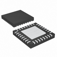
MAX8744AETJ+ Maxim Integrated Products, MAX8744AETJ+ Datasheet - Page 8

MAX8744AETJ+
Manufacturer Part Number
MAX8744AETJ+
Description
IC CNTRLR PWR SUP QUAD 32TQFN
Manufacturer
Maxim Integrated Products
Datasheet
1.MAX8744AETJ.pdf
(36 pages)
Specifications of MAX8744AETJ+
Applications
Controller, Notebook Computers
Voltage - Input
6 ~ 26 V
Number Of Outputs
4
Voltage - Output
3.3V, 5V, 1 ~ 26 V
Operating Temperature
0°C ~ 85°C
Mounting Type
Surface Mount
Package / Case
32-TQFN Exposed Pad
Lead Free Status / RoHS Status
Lead free / RoHS Compliant
High-Efficiency, Quad-Output, Main Power-
Supply Controllers for Notebook Computers
ELECTRICAL CHARACTERISTICS (continued)
(Circuit of Figure 1, V
no load, T
Note 1: The MAX8744A/MAX8745A cannot operate over all combinations of frequency, input voltage (V
Note 2: When the inductor is in continuous conduction, the output voltage has a DC-regulation level lower than the error-comparator
Note 3: Specifications from -40°C to +85°C are guaranteed by design, not production tested.
8
FAULT DETECTION
Output Overvoltage Trip
Threshold (MAX8744A Only)
Output Undervoltage Protection
PGOOD_ Lower Trip Threshold
PGOOD_ Output Low Voltage
GATE DRIVERS
DH_ Gate-Driver On-Resistance
DL_ Gate-Driver On-Resistance
INPUTS AND OUTPUTS
SHDN Input Trip Level
ONA Logic Input Voltage
ON3, ON5 Input Voltage
Tri-Level Input Logic
_______________________________________________________________________________________
large input-to-output differentials and high switching-frequency settings, the required on-time may be too short to maintain
the regulation specifications. Under these conditions, a lower operating frequency must be selected. The minimum on-time
must be greater than 150ns, regardless of the selected switching frequency. On-time and off-time specifications are mea-
sured from 50% point to 50% point at the DH_ pin with LX_ = GND, V
DH_ to LX_. Actual in-circuit times may differ due to MOSFET switching speeds.
threshold by 50% of the ripple. In discontinuous conduction (SKIP = GND, light load), the output voltage has a DC regula-
tion level higher than the trip level by approximately 1.1% due to slope compensation.
A
PARAMETER
= -40°C to +85°C, unless otherwise noted.) (Note 3)
IN
= 12V, both SMPS enabled, FSEL = REF, SKIP = GND, ILIM = LDO5, FBA = LDO5, I
SYMBOL
R
R
DH
DL
With respect to error comparator threshold
With respect to error comparator threshold
With respect to error comparator threshold,
hysteresis = 1%
I
BST_ – LX_ forced to 5V
DL_, high state
DL_, low state
Rising trip level
Falling trip level
Hysteresis = 600mV
SMPS off level/clear fault level
Delay start level
SMPS on level
SKIP, FSEL
SINK
= 1mA
CONDITIONS
BST_
High
Low
High
REF
GND
= 5V, and a 250pF capacitor connected from
V
0.96
1.65
MIN
-12
1.0
2.4
1.9
2.4
65
LDO5
8
IN
- 0.4
), and output voltage. For
TYP
REF
= I
MAX
LDO5
1.04
2.35
0.4
2.3
0.8
0.8
2.1
0.5
14
75
-8
5
5
3
= I
UNITS
OUTA
%
%
%
Ω
Ω
V
V
V
V
V
=


