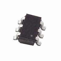
ZXSC420E6TA Diodes Zetex, ZXSC420E6TA Datasheet - Page 4

ZXSC420E6TA
Manufacturer Part Number
ZXSC420E6TA
Description
IC CONVERTER BOOST SOT23-6
Manufacturer
Diodes Zetex
Type
Step-Up (Boost)r
Datasheet
1.ZXSC410E6TA.pdf
(12 pages)
Specifications of ZXSC420E6TA
Internal Switch(s)
No
Synchronous Rectifier
No
Number Of Outputs
1
Voltage - Output
Adjustable
Current - Output
300mA
Frequency - Switching
Up to 200kHz
Voltage - Input
1.8 ~ 8 V
Operating Temperature
-40°C ~ 85°C
Mounting Type
Surface Mount
Package / Case
SOT-23-6
Power - Output
450mW
Lead Free Status / RoHS Status
Lead free / RoHS Compliant
Other names
ZXSC420E6TATR
Available stocks
Company
Part Number
Manufacturer
Quantity
Price
Part Number:
ZXSC420E6TA
Manufacturer:
ZETEX
Quantity:
20 000
DEVICE DESCRIPTION
Bandgap Reference
All threshold voltages and internal currents are derived
from a temperature compensated bandgap reference
circuit with a reference voltage of 1.22V nominal.
Dynamic Drive Output
Depending on the input signal, the output is either
“LOW” or “HIGH”. In the high state a 2.5mA current
source (max drive voltage = VCC-0.4V) drives the base
or gate of the external transistor. In order to operate the
external switching transistor at optimum efficiency,
both output states are initiated with a short transient
current in order to quickly discharge the base or the
gate of the switching transistor.
Switching Circuit
The switching circuit consists of two comparators,
Comp1 and Comp2, a gate U1, a monostable and the
drive output. Normally the DRIVE output is “HIGH”; the
external switching transistor is turned on. Current
ramps up in the inductor, the switching transistor and
external current sensing resistor. This voltage is
sensed by comparator, Comp2, at input I
the current sense voltage across the sensing resistor
exceeds 20mV, comparator Comp2 through gate U1
triggers a re-triggerable monostable and turns off the
output drive stage for 2µs. The inductor discharges to
the load of the application. After 2µs a new charge cycle
begins, thus ramping the output voltage. When the
output voltage reaches the nominal value and V
an input voltage of more than 300mV, the monostable
is forced “on” from Comp1 through gate U1, until the
feedback voltage falls below 300mV. The above action
continues to maintain regulation.
EOR, End of Regulation Detector
The EOR circuit is a retriggerable 120µs monostable,
which is re-triggered by every down regulating action
of comparator Comp1. As long as regulation takes
place, output EOR is “HIGH“ (high impedance, 100K to
V
120µs are ignored. If the output voltage falls below the
nominal value for more than 120µs, output EOR goes
”LOW“. The reason for this to happen is usually a
slowly progressing drop of input voltage from the
discharging battery. Therefore the output voltage will
also start to drop slowly. With the EOR detector,
batteries can be used to the ultimate end of discharge,
with enough time left for a safe shutdown.
ZXSC410
ZXSC420
CC
). Short dips of the output voltage of less than
S E M I C O N D U C T O R S
SENSE
FB
. Once
gets
4
Block Diagrams
STDN
R1
R2
R3
GND V
Shutdown
FB
SENSE
+
Comp 1
_
+
Comp 2
_
Fig. 1 ZXSC410
Fig. 1 ZXSC420
Bandgap
Reference
VCC
U1
Bias Generator
Monostable
2µs
ISSUE 2 - May 2003
Dynamic
Drive
DRIVE


