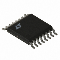
LT3439EFE#PBF Linear Technology, LT3439EFE#PBF Datasheet - Page 8

LT3439EFE#PBF
Manufacturer Part Number
LT3439EFE#PBF
Description
IC PUSH-PULL CNTRLR SYNC 16TSSOP
Manufacturer
Linear Technology
Type
Push-Pull Controllerr
Datasheet
1.LT3439EFEPBF.pdf
(12 pages)
Specifications of LT3439EFE#PBF
Internal Switch(s)
Yes
Synchronous Rectifier
No
Number Of Outputs
1
Current - Output
1A
Frequency - Switching
20kHz ~ 250kHz
Voltage - Input
2.8 ~ 17.5 V
Operating Temperature
-40°C ~ 125°C
Mounting Type
Surface Mount
Package / Case
16-TSSOP Exposed Pad, 16-eTSSOP, 16-HTSSOP
Primary Input Voltage
17.5V
No. Of Outputs
1
Output Voltage
35V
Output Current
1A
No. Of Pins
16
Operating Temperature Range
-40°C To +125°C
Msl
MSL 1 - Unlimited
Rohs Compliant
Yes
Pin Count
16
Input Voltage
17.5V
Switching Freq
20 to 250KHz
Package Type
TSSOP EP
Output Type
Adjustable
Switching Regulator
Yes
Mounting
Surface Mount
Input Voltage (min)
2.8V
Operating Temp Range
-40C to 125C
Operating Temperature Classification
Automotive
Lead Free Status / RoHS Status
Lead free / RoHS Compliant
Voltage - Output
-
Power - Output
-
Lead Free Status / Rohs Status
Compliant
Available stocks
Company
Part Number
Manufacturer
Quantity
Price
LT3439
APPLICATIO S I FOR ATIO
mean greater switching losses in the internal output
switches. However, efficiency is only modestly reduced
for a large improvement in EMI.
Care should be taken to ensure that the worst-case input
voltage and load current conditions do not cause an
excessive die temperature. The total power dissipation of
the IC is dominated by three loss terms, regulator losses,
saturation losses and switching losses. The following
formulas may be used to approximate these losses:
1. Regulator Dissipation:
2. Switch Saturation Dissipation:
3. Switch Switching Dissipation:
Total IC power dissipation (P
terms. Die junction temperature can be computed as
follows:
where T
temperature and
tion to ambient.
The LT3439 comes in the 16-pin TSSOP with exposed
backside package that has a very low junction-to-ambient
thermal resistance (
Transformer Design
Table 1 lists recommended center tapped transformers for
a variety of input voltage, output voltage and power
combinations.
8
P
SW
where I is the average switch current.
P
T
P
J
VIN
VSAT
= T
10
AMB
AMB
= (V
V
–
6
IN
is the ambient temperature, T
•
+ (P
SAT
V
12
IN
)(I)
mA
D
• •
JA
)(
I f
U
is the thermal resistance from junc-
JA
JA
OSC
60
) of approximately 40 C/W.
)
I
U
– . •
1 7 10
– . •
D
2 3 10
) is the sum of these three
W
–
3
–
V
4
•
I
R
•
J
R
SL
is the junction
SL
U
65 8
10 8
.
.
Table 1
These transformers will yield slightly high output voltages
so that they can accommodate an LDO regulator on the
output.
If your application is not listed, the LTC Applications group
is available to assist in the choice and/or the design of the
transformer.
In the design/selection of the transformer the following
characteristics are critical and should be considered.
Turns Ratio
The turns ratio of the transformer determines the output
voltage. The following equation can be used as a first pass
to calculate the turns ratio:
where V
V
Typical Performance curves).
Sufficient margin should be added to the turns ratio to
account for voltage drops due to transformer winding
resistances. Also, if using an LDO for regulating the output
voltage, don’t forget to take into account the voltage drop
that should be added to V
Magnetizing Current
The primary inductance of the transformer causes a ripple
current that is independent of load current. The ripple
current manifests itself in the output voltage through the
parasitic resistances of the supply. Increasing the trans-
former magnetizing inductance can reduce the ripple
SW
NOMINAL
VOLTAGE
N
N
INPUT
P
S
is the voltage drop across the internal switches (see
12V
5V
5V
5V
5V
5V
5V
F
V
V
is the forward voltage of the output diode and
IN
OUT
–
V
SW
NOMINAL
VOLTAGE
V
OUTPUT
F
–12V
12V
12V
12V
12V
15V
15V
OUT
.
OUTPUT
POWER
1.5W
3.0W
1.5W
3.0W
1.5W
10W
6W
CTX02-13716-X1
CTX02-13665-X1
CTX02-13713-X1
CTX02-13664-X1
CTX02-13834-X3
CTX02-13949-X1
PART NUMBER
COILTRONICS
CTX02-16076
sn3439 3439fs


