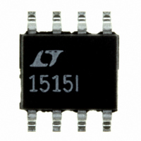
LTC1515IS8#PBF Linear Technology, LTC1515IS8#PBF Datasheet - Page 5

LTC1515IS8#PBF
Manufacturer Part Number
LTC1515IS8#PBF
Description
IC MULTI CONFIG ADJ 50MA 8SOIC
Manufacturer
Linear Technology
Type
Step-Down (Buck), Step-Up (Boost), Switched Capacitor (Charge Pump)r
Datasheet
1.LTC1515IS8PBF.pdf
(8 pages)
Specifications of LTC1515IS8#PBF
Internal Switch(s)
Yes
Synchronous Rectifier
No
Number Of Outputs
1
Voltage - Output
Adjustable
Current - Output
50mA
Frequency - Switching
650kHz
Voltage - Input
2 ~ 10 V
Operating Temperature
-40°C ~ 85°C
Mounting Type
Surface Mount
Package / Case
8-SOIC (3.9mm Width)
Lead Free Status / RoHS Status
Lead free / RoHS Compliant
Power - Output
-
Available stocks
Company
Part Number
Manufacturer
Quantity
Price
SI PLIFIED
C1
Terminal.
V
2V and 10V. V
ESR capacitor as close as possible to the pin for best
performance.
PIN
APPLICATIONS
Regulator Operation
The regulator section of the LTC1515, LTC1515-3/5 and
LTC1515-3.3/5 consists of a charge pump, reference,
comparator and some logic. The divided down output
voltage is compared to the internal reference voltage.
When the divided output drops below the reference volt-
age, the charge pump is enabled, which boosts the output
back into regulation. Hysteresis in the comparator forces
the regulator to burst on and off and causes approximately
100mV of peak-to-peak ripple to appear at the output. By
enabling the charge pump only when needed, the parts
achieve high efficiencies with low output load currents.
IN
+
W
U
(Pin 7): Charge Pump Input Voltage. May be between
(Pin 6): Charge Pump Flying Capacitor, Positive
FUNCTIONS
U
IN
should be bypassed with a
SHDN
POR
V
BLOCK
U
IN
U
INFORMATION
U
DIGRAM
W
OSCILLATOR
COUNTER
650kHz
RESET
W
U
10 F low
EN
EN
STEP-UP/STEP-DOWN
C1
CHARGE PUMP
–
Each part’s charge pump has a unique architecture that
allows the input voltage to be either stepped up or stepped
down to produce a regulated output. Internal circuitry
senses the V
charge pump operating mode. In addition, the effective
output impedance of the charge pump is internally
adjusted to prevent large inrush currents and allow for a
wide input voltage range. When the input voltage is lower
than the output voltage, the charge pump operates as a
step-up voltage doubler. When the input voltage is greater
than the output, the charge pump operates as a step-down
gated switch.
V
either 3V/5V, 3.3V/5V or adjustable using an external
resistor divider (LTC1515). V
a 10 F low ESR capacitor as close as possible to the pin
for best performance.
OUT
–
+
–
+
(Pin 8): Regulated Output Voltage. Pin selectable to
C1
V
OS
+
1.232V
IN
(LTC1515-X)
V
(LTC1515-X)
REF
to V
GND
OUT
LTC1515 • BD
differential voltage and controls the
OUT
LTC1515 Series
FB
(LTC1515)
5/3
(LTC1515-X)
V
should be bypassed with
OUT
5


