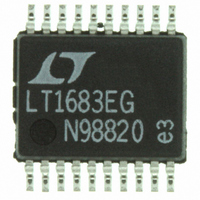
LT1738EG#PBF Linear Technology, LT1738EG#PBF Datasheet - Page 18

LT1738EG#PBF
Manufacturer Part Number
LT1738EG#PBF
Description
IC DC/DC CONTRLR LOW NOIS 20SSOP
Manufacturer
Linear Technology
Type
Step-Up (Boost), Cuk, Flybackr
Datasheet
1.LT1738EGPBF.pdf
(20 pages)
Specifications of LT1738EG#PBF
Internal Switch(s)
No
Synchronous Rectifier
No
Number Of Outputs
1
Voltage - Output
5 ~ 100 V
Frequency - Switching
20kHz ~ 250kHz
Voltage - Input
2.55 ~ 20 V
Operating Temperature
-40°C ~ 125°C
Mounting Type
Surface Mount
Package / Case
20-SSOP
Lead Free Status / RoHS Status
Lead free / RoHS Compliant
Current - Output
-
Power - Output
-
Available stocks
Company
Part Number
Manufacturer
Quantity
Price
APPLICATIO S I FOR ATIO
LT1738
First determine the maximum gate drive that you require.
Typically you will want it to be at least 2V greater than the
rated threshold. Higher voltages will lower the on resis-
tance and increase efficiency. Be certain to check the
maximum allowed gate voltage. Often this is 20V but for
some logic threshold MOSFETs it is only 8V to 10V.
V
max gate threshold. In addition V
1.6V above the gate voltage.
The GCL pin can be tied to V
maximum gate voltage of V
This pin also controls undervoltage lockout of the gate
drive. The undervoltage lockout will prevent the MOSFET
from switching until there is sufficient drive present.
If GCL is tied to a voltage source or zener less than 6.8V,
the gate drivers will not turn on until V
voltage by 0.8V. For V
insured to be off for V
by V
If GCL is tied to V
(undervoltage lockout is disabled).
Approximately 50 A of current can be sourced from this
pin if V
The GCL pin has an internal 19V zener to ground that will
provide a failsafe for maximum gate voltage.
As an example say we are using a Siliconix Si4480DY
which has R
be set to 6.2V and V
Gate Driver Considerations
In general, the MOSFET should be positioned as close to
the part as possible to minimize inductance.
When the part is active the gate drive will be pulled low to
less than 0.2V. When the part is off, the gate drive contains
a 40k resistor in series with a diode to ground that will offer
passive holdoff protection. If you are using some logic
level MOSFETs this might not be sufficient. A resistor may
be placed from gate to ground, however the value should
be reasonably high to minimize DC losses and possible AC
issues.
18
GCL
GCL
needs to be set approximately 0.2V above the desired
IN
+ 0.8V.
> V
GCL
DS(ON)
+ 0.8V. This could be used to bias a zener.
rated at 6V. To get 6V, V
U
IN
IN
IN
needs to be at least 7.6V.
GCL
, the gate driver is always on
< 7.3V and they will be turned on
U
above 6.5V, the gate drive is
IN
– 1.6V.
IN
IN
which will result in a
W
needs to be at least
IN
exceeds the GCL
GCL
U
needs to
The gate drive source current comes from V
current exits through PGND. In general the decoupling cap
should be placed close to these two pins.
Switching Diodes
In general, switching diodes should be Schottky diodes.
Size and breakdown voltage depend on the specific con-
verter. A lower forward drop will improve converter effi-
ciency. No other special requirements are needed.
PCB LAYOUT CONSIDERATIONS
As with any switcher, careful consideration should be given
to PC board layout. Because this part reduces high fre-
quency EMI, the board layout is less critical. However, high
currents and voltages still produce the need for careful
board layout to eliminate poor and erratic performance.
Basic Considerations
Keep the high current loops physically small in area. The
main loops are shown in Figure 6: the power switch loops
(A) and the rectifier loop (B). These loops can be kept small
by physically keeping the components close to one an-
other. In addition, connection traces should be kept wide
to lower resistance and inductances. Components should
be placed to minimize connecting paths. Careful attention
to ground connections must also be maintained. Be care-
ful that currents from different high current loops do not
get coupled into the ground paths of other loops. Using
singular points of connection for the grounds is the best
way to do this. The two major points of connection are the
bottom of the input decoupling capacitor and the bottom
of the output decoupling capacitor. Typically, the sense
resistor device PGND and device GND will tie to the bottom
of the input capacitor.
V
IN
C
IN
GATE
A
CS
Figure 6
•
•
B
C
OUT
IN
. The sink
1738 F06
V
OUT
1738fa


