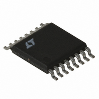
LT3431EFE#PBF Linear Technology, LT3431EFE#PBF Datasheet - Page 9

LT3431EFE#PBF
Manufacturer Part Number
LT3431EFE#PBF
Description
IC SW REG STEP-DOWN 3A 16TSSOP
Manufacturer
Linear Technology
Type
Step-Down (Buck)r
Datasheet
1.LT3431EFEPBF.pdf
(28 pages)
Specifications of LT3431EFE#PBF
Internal Switch(s)
Yes
Synchronous Rectifier
No
Number Of Outputs
1
Voltage - Output
1.2 ~ 48 V
Current - Output
3A
Frequency - Switching
500kHz
Voltage - Input
5.5 ~ 60 V
Operating Temperature
-40°C ~ 125°C
Mounting Type
Surface Mount
Package / Case
16-TSSOP Exposed Pad, 16-eTSSOP, 16-HTSSOP
Primary Input Voltage
60V
No. Of Outputs
1
Output Voltage
48V
Output Current
6.5A
No. Of Pins
16
Operating Temperature Range
-40°C To +125°C
Msl
MSL 1 - Unlimited
Rohs Compliant
Yes
Lead Free Status / RoHS Status
Lead free / RoHS Compliant
Power - Output
-
Available stocks
Company
Part Number
Manufacturer
Quantity
Price
APPLICATIO S I FOR ATIO
will increase and the protection accorded by frequency
and current foldback will decrease.
CHOOSING THE INDUCTOR
For most applications, the output inductor will fall into the
range of 5 H to 33 H. Lower values are chosen to reduce
physical size of the inductor. Higher values allow more
output current because they reduce peak current seen by
the LT3431 switch, which has a 3A limit. Higher values
also reduce output ripple voltage.
When choosing an inductor you will need to consider
output ripple voltage, maximum load current, peak induc-
tor current and fault current in the inductor. In addition,
other factors such as core and copper losses, allowable
component height, EMI, saturation and cost should also
be considered. The following procedure is suggested as a
way of handling these somewhat complicated and con-
flicting requirements.
Output Ripple Voltage
Figure 3 shows a comparison of output ripple voltage for
the LT3431 using either a tantalum or ceramic output
capacitor. It can be seen from Figure 3 that output ripple
voltage can be significantly reduced by using the ceramic
output capacitor; the significant decrease in output ripple
voltage is due to the very low ESR of ceramic capacitors.
U
LT3431
V
U
C
Q2
GND
AMPLIFIER
W
TO SYNC CIRCUIT
ERROR
Figure 2. Frequency and Current Limit Foldback
TO FREQUENCY
SHIFTING
+
–
U
1.4V
1.2V
R3
1k
BUFFER
Q1
R4
2k
Output ripple voltage is determined by ripple current
(I
impedance of the output capacitor. At high frequencies,
the impedance of the tantalum capacitor is dominated by
its effective series resistance (ESR).
Tantalum Output Capacitor
The typical method for reducing output ripple voltage
when using a tantalum output capacitor is to increase the
inductor value (to reduce the ripple current in the induc-
tor). The following equations will help in choosing the
required inductor value to achieve a desirable output
ripple voltage level. If output ripple voltage is of less
LP-P
10mV/DIV
Figure 3. LT3431 Output Ripple Voltage Waveforms.
Ceramic vs Tantalum Output Capacitors
) through the inductor and the high frequency
V
V
L = 10 H
IN
OUT
= 12V
V
= 5V
SW
FB
L1
R1
R2
+
1 s/DIV
3431 F02
C1
OUTPUT
5V
3431 F03
LT3431
V
47 F CERAMIC
OUTPUT
CAPACITOR
V
100 F, 0.08
TANTALUM
OUTPUT
CAPACITOR
OUT
OUT
USING
USING
sn3431 3431fs
9


