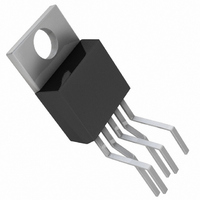
LT1074CT#PBF Linear Technology, LT1074CT#PBF Datasheet - Page 12

LT1074CT#PBF
Manufacturer Part Number
LT1074CT#PBF
Description
IC MULTI CONFIG ADJ 5A TO220-5
Manufacturer
Linear Technology
Type
Step-Down (Buck), Step-Up (Boost), Inverting, Flybackr
Datasheet
1.LT1076CTPBF.pdf
(16 pages)
Specifications of LT1074CT#PBF
Internal Switch(s)
Yes
Synchronous Rectifier
No
Number Of Outputs
1
Voltage - Output
2.5 ~ 50 V
Current - Output
5A
Frequency - Switching
100kHz
Voltage - Input
8 ~ 45 V
Operating Temperature
0°C ~ 70°C
Mounting Type
Through Hole
Package / Case
TO-220-5 (Bent and Staggered Leads)
Dc To Dc Converter Type
Step Down
Pin Count
5 +Tab
Input Voltage
45V
Output Voltage
2.5 to 50V
Switching Freq
125kHz
Output Current
10A
Package Type
TO-220
Output Type
Adjustable
Switching Regulator
Yes
Line Regulation
0.02%/V
Mounting
Through Hole
Input Voltage (min)
8V
Operating Temperature Classification
Commercial
Primary Input Voltage
60V
No. Of Outputs
1
No. Of Pins
5
Operating Temperature Range
0°C To +125°C
Msl
MSL 1 - Unlimited
Supply Voltage Range
8V To 40V
Rohs Compliant
Yes
Lead Free Status / RoHS Status
Lead free / RoHS Compliant
Power - Output
-
Lead Free Status / Rohs Status
Compliant
Available stocks
Company
Part Number
Manufacturer
Quantity
Price
LT1074/LT1076
PI
Phase shift from the FB pin to the V
frequencies where the external C
drops back to 0° (actually 180° since FB is an inverting
input) when the reactance of C
The low frequency “pole” where the reactance of C
equal to the output impedance of Q4 and Q6 (r
Although f
mid-frequency gain is dependent only on G
specified much tighter on the data sheet. The higher
frequency “zero” is determined solely by R
12
A
A
f
f
U
POLE
ZERO
V
V
=
=
DESCRIPTIO S
G
2π
=
=
POLE
m
2
2π
• •
G
•
π
f C
R at high frequencies
m
•
•
varies as much as 3:1 due to r
C
1
r
R
O
1
C
C
•
•
C
at mid frequencies
C
r
O
C
≈
U
400
90 A
C
µ
2.21V
k
C
is small compared to R
Ω
is controlling gain, then
X1.8
ALL CURRENTS SHOWN ARE AT NULL CONDITION
Q1
C
pin is 90° at mid
140 A
Q2
µ
C
O
50 A
and C
m
µ
variations,
, which is
O
Figure 10. Error Amplifier
), is:
FB
C
.
C
Q3
300
C
is
D2
50 A
.
µ
Ω
D1
The error amplifier has asymmetrical peak output current.
Q3 and Q4 current mirrors are unity-gain, but the Q6
mirror has a gain of 1.8 at output null and a gain of 8 when
the FB pin is high (Q1 current = 0). This results in a
maximum positive output current of 140µA and a maxi-
mum negative (sink) output current of ≅1.1mA. The asym-
metry is deliberate—it results in much less regulator
output overshoot during rapid start-up or following the
release of an output overload. Amplifier offset is kept low
by area scaling Q1 and Q2 at 1.8:1.
Amplifier swing is limited by the internal 5.8V supply for
positive outputs and by D1 and D2 when the output goes
low. Low clamp voltage is approximately one diode drop
(≈0.7V – 2mV/°C).
Note that both the FB pin and the V
connections. Refer to the frequency shifting and synchro-
nizing discussions.
Q4
Q6
90 A
90 A
V
5.8V
µ
µ
C
R
C
C
C
EXTERNAL
FREQUENCY
COMPENSATION
LT1074 • PD11
C
pin have other internal
sn1074 1074fds


