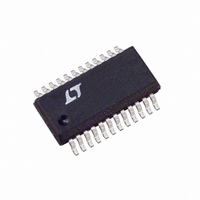
LTC1436AIGN-PLL#PBF Linear Technology, LTC1436AIGN-PLL#PBF Datasheet - Page 21

LTC1436AIGN-PLL#PBF
Manufacturer Part Number
LTC1436AIGN-PLL#PBF
Description
IC SW REG SYNC STEP-DOWN 24-SSOP
Manufacturer
Linear Technology
Type
Step-Down (Buck)r
Datasheet
1.LTC1436AIGN-PLLPBF.pdf
(28 pages)
Specifications of LTC1436AIGN-PLL#PBF
Internal Switch(s)
No
Synchronous Rectifier
Yes
Number Of Outputs
1
Voltage - Output
1.19 ~ 9 V
Current - Output
50mA
Frequency - Switching
125kHz ~ 240kHz
Voltage - Input
3.5 ~ 30 V
Operating Temperature
-40°C ~ 85°C
Mounting Type
Surface Mount
Package / Case
24-SSOP
Lead Free Status / RoHS Status
Lead free / RoHS Compliant
Power - Output
-
Available stocks
Company
Part Number
Manufacturer
Quantity
Price
Part Number:
LTC1436AIGN-PLL#PBFLTC1436AIGN-PLL
Manufacturer:
Linear Technology
Quantity:
135
APPLICATIONS
Efficiency Considerations
The efficiency of a switching regulator is equal to the
output power divided by the input power times 100%. It is
often useful to analyze individual losses to determine what
is limiting the efficiency and which change would produce
the most improvement. Efficiency can be expressed as:
where L1, L2, etc. are the individual losses as a percentage
of input power.
Although all dissipative elements in the circuit produce
losses, four main sources usually account for most of the
losses in LTC1436A/LTC1437A circuits: LTC1436A/
LTC1437A V
topside MOSFET transition losses.
1. The V
2. INTV
Efficiency = 100% – (L1 + L2 + L3 + ...)
Electrical Characteristics table which excludes MOSFET
driver and control currents. V
small (< 1%) loss which increases with V
control currents. The MOSFET driver current results
from switching the gate capacitance of the power
MOSFETs. Each time a MOSFET gate is switched from
low to high to low again, a packet of charge dQ moves
from INTV
out of INTV
control circuit current. In continuous mode, I
f(Q
topside and bottom side MOSFETs. It is for this reason
that the Adaptive Power output stage switches to a low
Q
By powering EXTV
the additional V
control currents will be scaled by a factor of Duty Cycle/
Figure 13. Allowable Inductor/R
T
T
MOSFET during low current operation.
+ Q
CC
IN
B
current is the sum of the MOSFET driver and
current is the DC supply current given in the
), where Q
IN
CC
CC
current, INTV
to ground. The resulting dQ/dt is a current
that is typically much larger than the
IN
U
current resulting from the driver and
CC
T
and Q
INFORMATION
from an output-derived source,
U
L
B
CC
are the gate charges of the
SENSE
1435A F08
current, I
INDUCTOR
IN
W
Layout Orientations
current results in a
2
R losses and
IN
.
U
GATECHG
=
3. I
4. Transition losses apply only to the topside MOSFET(s),
Other losses including C
losses, Schottky conduction losses during dead-time and
inductor core losses, generally account for less than 2%
total additional loss.
Checking Transient Response
The regulator loop response can be checked by looking at
the load transient response. Switching regulators take
several cycles to respond to a step in DC (resistive) load
current. When a load step occurs, V
by an amount equal to (∆I
effective series resistance of C
charge or discharge C
error signal. The regulator loop then acts to return V
its steady-state value. During this recovery time V
be monitored for overshoot or ringing, which would
indicate a stability problem. The I
shown in the Figure 1 circuit will provide adequate com-
pensation for most applications.
Efficiency. For example, in a 20V to 5V application,
10mA of INTV
of V
10% or more (if the driver was powered directly from
V
MOSFET, inductor and current shunt. In continuous
mode the average output current flows through L and
R
MOSFET and the synchronous MOSFET. If the two
MOSFETs have approximately the same R
the resistance of one MOSFET can simply be summed
with the resistances of L and R
losses. For example, if each R
R
tance is 0.25Ω. This results in losses ranging from 3%
to 10% as the output current increases from 0.5A to 2A.
I
currents.
and only when operating at high input voltages (typi-
cally 20V or greater). Transition losses can be esti-
mated from:
Transition Loss = 2.5(V
2
2
IN
SENSE
L
R losses are predicted from the DC resistances of the
R losses cause the efficiency to drop at high output
) to only a few percent.
= 0.15Ω and R
IN
current. This reduces the midcurrent loss from
, but is “chopped” between the topside main
LTC1436A-PLL/LTC1437A
CC
current results in approximately 3mA
SENSE
OUT
IN
IN
LOAD
= 0.05Ω, then the total resis-
which generates a feedback
)
1.85
and C
OUT
)(ESR), where ESR is the
(I
TH
. ∆I
MAX
OUT
OUT
external components
SENSE
LOAD
)(C
immediately shifts
DS(ON)
LTC1436A
ESR dissipative
RSS
also begins to
to obtain I
DS(ON)
)(f)
= 0.05Ω,
OUT
21
OUT
, then
14367afb
can
2
to
R


