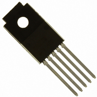
BD9870FPS-E2 Rohm Semiconductor, BD9870FPS-E2 Datasheet

BD9870FPS-E2
Specifications of BD9870FPS-E2
Available stocks
Related parts for BD9870FPS-E2
BD9870FPS-E2 Summary of contents
Page 1
... BD9870FPS ● Description The BD9870FPS single-channel step-down switching regulator incorporates a Pch MOSFET capable of PWM operation at 900kHz, enabling use of a smaller coil, as well as circuitry that eliminates the need for external compensation – only a diode, coil, and ceramic capacitor are required – reducing board size significantly. ...
Page 2
... BD9870FPS ●Electrical Characteristics(Unless otherwise noted, Ta=25℃,Vcc=12V,Vo=5V,STBY=3V) Parameter Output ON Resistance Efficiency Switching Frequency Load Regulation Line Regulation Over Current ProtectionLimit INV Pin Threshold Voltage INV Pin Input Current ON STBY Pin Threshold Voltage OFF STBYPin Input Current Circuit Current ...
Page 3
... BD9870FPS ●Package Dimensions Fig.2 ●Pin Description Pin No. Pin Name 1 VCC 2 OUT 3 ※ OUT FIN GND 4 INV 5 STBY ※Normally OPEN www.rohm.com © 2009 ROHM Co., Ltd. All rights reserved. TO252S-5(Unit:mm) Function Input Power Supply Pin Internal Pch FET Drain Pin ...
Page 4
... BD9870FPS ●Block Function Explanations ・ VREF Generates the regulated voltage from Vcc input, compensated for temperature. ・ OSC Generates the triangular wave oscillation frequency (900kHz) using an internal resistors and capacitor. Used for PWM comparator input. ・ Error AMP This block, via the INV pin, detects the resistor-divided output voltage, compares this with the reference voltage, then amplifies and outputs the difference. ・ ...
Page 5
... BD9870FPS ●Application component selection and settings Inductor L1 A large inductor series impedance will result in deterioration of efficiency. OCP operation greater than 1.6A may cause inductor overheating, possibly leading to overload or output short. Note that the current rating for the coil should be higher than I Iout( ...
Page 6
... BD9870FPS <Recommended Components (Example)> Inductor L1=10μH Schottky Diode D1 D2 Capacitor C1=10μF(25V) :ceramic cap GRM31CB31E106KA75L(murata) C2=4.7μF(50V) :ceramic cap GRM32EB31H475KA87L(murata) C3=OPEN <Recommended Components example 2>…when the Duty ratio of output/input voltage is less than 10% Inductor L1=10μH Schottky Diode D1 D2 Capacitor C1= ...
Page 7
... BD9870FPS ●Typical Performance Characteristics(Unless otherwise noted, Ta=25℃,Vcc=12V,Vo=5V,STBY=3V) Input Voltage[V] Fig.5 Circuit Current vs. Supply Voltage:no load 1100 1050 1000 950 900 850 800 750 700 Input Voltage[V] Fig.7 Oscillator Frequency vs. Supply Voltage 1.05 1.04 1.03 1.02 1.01 1 ...
Page 8
... BD9870FPS 3.0 2.5 2.0 1.5 1.0 0.5 0.0 0.0 0.5 1.0 Output Current[A] Fig.11 Driver Drain-Source Voltage vs. Output Current Input Voltage[V] Fig.13 Output Voltage vs. Supply Voltage 6.0 5.5 5.0 4.5 4.0 3.5 3.0 2.5 2.0 1.5 1.0 0.5 0.0 0.0 0.5 1 ...
Page 9
... BD9870FPS ●I/O Equivalent Circuit Pin 1 (Vcc, GND) VCC OUT GND ●Operation Notes 1. Absolute Maximum Ratings Exceeding the absolute maximum ratings (i.e. supply voltage, temperature) may cause damage to the device and make it impossible to determine the failure mode (short/open). Therefore, when conditions exceeding the maximum ratings are anticipated, consideration should be given to preventive countermeasures (e ...
Page 10
... BD9870FPS 10. This monolithic IC which (as below) has P+ substrate and between the various pin. A P-N junction is formed from this P layer of each pin. For example the relation between each potential is as follows.(When GND > PinB and GND > PinA, the P-N junction operates as a parasitic diode.) Parasitic diodes can occur inevitably in the structure of the IC ...
Page 11
... BD9870FPS ●Ordering part number Part No. Part No. TO252S-5 1.2±0.1 6.5±0.2 0.27±0.1 C0.5 +0.2 5.1 −0.1 FIN 0.71 0.27±0.1 0.6±0.2 S 0.08 M 0.27±0.1 1.27 0.08 S www.rohm.com © 2009 ROHM Co., Ltd. All rights reserved Package FPS = TO252S-5 <Tape and Reel information> ...
Page 12
No copying or reproduction of this document, in part or in whole, is permitted without the consent of ROHM Co.,Ltd. The content specified herein is subject to change for improvement without notice. The content specified herein is for the purpose ...


