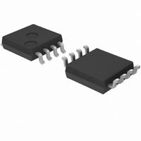
BD9109FVM-TR Rohm Semiconductor, BD9109FVM-TR Datasheet - Page 18

BD9109FVM-TR
Manufacturer Part Number
BD9109FVM-TR
Description
IC REG SW 0.8A 3.3VOUTPUT 8-MSOP
Manufacturer
Rohm Semiconductor
Type
Step-Down (Buck)r
Series
-r
Datasheet
1.BD9106FVM-TR.pdf
(29 pages)
Specifications of BD9109FVM-TR
Internal Switch(s)
Yes
Synchronous Rectifier
Yes
Number Of Outputs
1
Voltage - Output
3.3V
Current - Output
800mA
Frequency - Switching
1MHz
Voltage - Input
4.5 ~ 5.5 V
Operating Temperature
-25°C ~ 85°C
Mounting Type
Surface Mount
Package / Case
8-MSOP, Micro8™, 8-uMAX, 8-uSOP,
Power - Output
587.4mW
Output Voltage
3.3 V
Output Current
0.8 A
Input Voltage
4.5 V to 5.5 V
Switching Frequency
1 MHz
Mounting Style
SMD/SMT
Lead Free Status / RoHS Status
Lead free / RoHS Compliant
Available stocks
Company
Part Number
Manufacturer
Quantity
Price
Company:
Part Number:
BD9109FVM-TR
Manufacturer:
JRC
Quantity:
4 301
Part Number:
BD9109FVM-TR
Manufacturer:
ROHM/罗姆
Quantity:
20 000
●Operation
© 2009 ROHM Co., Ltd. All rights reserved.
BD9106FVM,BD9107FVM,BD9109FVM,BD9110NV,BD9120HFN
Current
RESET
www.rohm.com
Comp
V
SET
SW
OUT
BD9106FVM,BD9107FVM,BD9109FVM,BD9110NV,BD9120HFN are a synchronous rectifying step-down switching
regulator that achieves faster transient response by employing current mode PWM control system. It utilizes switching
operation in PWM (Pulse Width Modulation) mode for heavier load, while it utilizes SLLM
operation for lighter load to improve efficiency.
○Synchronous rectifier
○Current mode PWM control
I
L
It does not require the power to be dissipated by a rectifier externally connected to a conventional DC/DC converter IC,
and its P.N junction shoot-through protection circuit limits the shoot-through current during operation, by which the
power dissipation of the set is reduced.
Synthesizes a PWM control signal with a inductor current feedback loop added to the voltage feedback.
・PWM (Pulse Width Modulation) control
・SLLM
receives two signals, a current feedback control signal (SENSE: Voltage converted from I
control signal (FB), and issues a RESET signal if both input signals are identical to each other, and turns OFF the
P-channel MOS FET (while a N-channel MOS FET is turned ON) for the rest of the fixed period. The PWM control
repeat this operation.
The oscillation frequency for PWM is 1 MHz. SET signal form OSC turns ON a P-channel MOS FET (while a
N-channel MOS FET is turned OFF), and an inductor current I
When the control mode is shifted from PWM for heavier load to the one for lighter load or vise versa, the switching
pulse is designed to turn OFF with the device held operated in normal PWM control loop, which allows linear
operation without voltage drop or deterioration in transient response during the mode switching from light load to
heavy load or vise versa.
Although the PWM control loop continues to operate with a SET signal from OSC and a RESET signal from Current
Comp, it is so designed that the RESET signal is held issued if shifted to the light load mode, with which the switching
is tuned OFF and the switching pulses are thinned out under control. Activating the switching intermittently reduces
the switching dissipation and improves the efficiency.
Fig.88 PWM switching timing chart
V
TM
OUT
(Simple Light Load Mode) control
Gm Amp.
Level
Shift
Fig.87 Diagram of current mode PWM control
ITH
FB
SENSE
Current
Comp
PVCC
GND
GND
GND
I
V
L
RESET
(AVE)
OUT
OSC
SET
(AVE)
FB
SENSE
R Q
S
18/28
Current
RESET
Comp
Driver
Logic
V
SET
SW
OUT
I
L
L
increases. The current comparator (Current Comp)
Fig.89 SLLM switching timing chart
SW
I
L
Not switching
TM
Load
(Simple Light Load Mode)
L
) and a voltage feedback
V
OUT
Technical Note
2009.05 - Rev.A
FB
PVCC
SENSE
GND
GND
GND
0A
V
OUT
(AVE)


