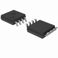
BD9850FVM-TR Rohm Semiconductor, BD9850FVM-TR Datasheet - Page 11

BD9850FVM-TR
Manufacturer Part Number
BD9850FVM-TR
Description
IC REG SW STEP DOWN HI EFF 8MSOP
Manufacturer
Rohm Semiconductor
Type
Step-Down (Buck)r
Series
-r
Datasheet
1.BD9850FVM-TR.pdf
(17 pages)
Specifications of BD9850FVM-TR
Internal Switch(s)
No
Synchronous Rectifier
No
Number Of Outputs
1
Current - Output
200mA
Frequency - Switching
100kHz ~ 2MHz
Voltage - Input
4 ~ 9 V
Operating Temperature
-40°C ~ 85°C
Mounting Type
Surface Mount
Package / Case
8-MSOP, Micro8™, 8-uMAX, 8-uSOP,
Power - Output
587mW
Mounting Style
SMD/SMT
Pwm Type
Controller
Frequency - Max
2MHz
Duty Cycle
-
Voltage - Supply
4 V ~ 9 V
Buck
Yes
Boost
No
Flyback
No
Inverting
No
Doubler
No
Divider
No
Cuk
No
Isolated
No
Lead Free Status / RoHS Status
Lead free / RoHS Compliant
Voltage - Output
-
Lead Free Status / Rohs Status
Lead free / RoHS Compliant
Available stocks
Company
Part Number
Manufacturer
Quantity
Price
Company:
Part Number:
BD9850FVM-TR
Manufacturer:
ST
Quantity:
110
Part Number:
BD9850FVM-TR
Manufacturer:
ROHM/罗姆
Quantity:
20 000
• Setting of oscillation frequency (BD9851EFV)
• Setting of timer of short circuit protection circuit (BD9851EFV)
Connecting a resistor to the RT pin (pin 2) and a capacitor to the CT pin allows
for the setting of oscillation frequency.
In order to use one channel, treat the pins of unused channel as shown above.
• Setting of maximum duty (BD9851EFV)
• Pin treatment of unused channels (BD9851EFV)
Fig. 22 Pin treatment procedure for unused channel on BD9851EFV
T
DUTY(max.) = 100 × (V
V
SCP
DTC
1000
1000
DUTY(max.)
V
Vth0
Vth100
100
O
DTC
10
T
= 7.45 × 10
= 2.5 × R2 / (R1 + R2)
SCP
SCP
1
Fig. 20 RT vs. Oscillation frequency
:
:
Time from output short circuit to latch stop [sec]
Capacitance of capacitor between the SCP and
GND pins [F]
Upper : Pin No. to be treated when the CH1 is not used
Lower : Pin No. to be treated when the CH2 is not used
SEL1
(18)
Vcc
(1)
C
C
CT
C
CT
=1200pF
CT
=220pF
5
NON2
=33pF
× C
: Maximum duty [%]
: DTC pin voltage [V]
: 0% duty threshold voltage [V]
: 100% duty threshold voltage [V]
(4)
Timing Resistance (kΩ)
SCP
Setting procedure
Setting procedure
V
(17)
(16)
INV
(5)
REF
DTC
– Vth0) / (Vth100 – Vth0)
10
(15)
FB
(6)
DTC
(13)
(7)
PVcc
(18)
(12)
Vcc
(8)
OUT
(11)
(9)
100
11/16 5
Fig. 19 Setting procedure for BD9851EFV oscillation frequency
1000
1000
100
C
10
SCP
10
R1
R2
Fig. 20 CT vs. Oscillation frequency
Application
Application
Timing Capacitance(pF)
V
SCP (14)
10
DTC (13)(7)
REF
R
C
RT
CT
(17)
100
R
R
RT
RT
RT (2)
CT (3)
=4.7kΩ
=24kΩ
1000


