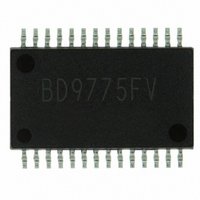
BD9775FV-E2 Rohm Semiconductor, BD9775FV-E2 Datasheet

BD9775FV-E2
Specifications of BD9775FV-E2
Related parts for BD9775FV-E2
BD9775FV-E2 Summary of contents
Page 1
... High Efficiency Step-down Switching Regulator Controller BD9775FV ●Description BD9775FV is Switching Controller with synchronous rectification (BD9775FV is 1channel synchronous rectification) and wide input range. It can contribute to ecological design (lower power consumption) for most of electronic equipments. ●Features 1) 2channel Step-Down DC/DC FET driver 2) Synchronous rectification for channel 2 ...
Page 2
... BD9775FV ●Electrical characteristics (Ta=25℃, VCC=13.2V, fosc=100kHz, CTL1=3V, CTL2=3V) Parameter 【Whole Device】 Stand-by Current Circuit Current 【Reference Voltage】 VREF Output Voltage Line Regulation Load Regulation Short Output Current 【Internal Voltage Regulator】 VREGA Output Voltage VREGB Output Voltage VREGB Dropout Voltage 【 ...
Page 3
... BD9775FV Parameter 【PWM Comparator】 Threshold Voltage at 0% Threshold Voltage at 100% DTC Input Bias Current 【FET Driver】 Sink Current Source Current ON Resistance Rise Time Fall Time Driver’s Duty Cycle of Synchronous Rectification SYNC Terminal Voltage 【Over Current Protection (OCP)】 ...
Page 4
... BD9775FV ●Pin Description FB1 1 INV1 2 RT PVCC1 3 CT OUT1 4 Fin VREGB 5 6 GND OUT2H VREF PVCC2 7 CL2 8 DTC1 9 VS2 DTC2 INV2 10 SCP VREGA 12 CTL1 OUT2L CTL2 13 PGND VCC SYNC 14 Fig.1 Pin Description ●Block Diagram Fig.2 Block Diagram www.rohm.com © 2011 ROHM Co., Ltd. All rights reserved. ...
Page 5
... BD9775FV ●Function Explanation 1. DC/DC Converter ・Reference Voltage Stable voltage of compensated temperature, is generated from the power supply voltage (VCC). The reference voltage is 3.0V, the accuracy is ±1%. Place a capacitor with low ESR (several decades mΩ) between VREF and GND. ・Internal Regulator A (VREGA generated the power supply voltage. The voltage is for the driver of the synchronous rectification’s MOSFET. ...
Page 6
... BD9775FV ●Setting Up Information 1) Simultaneously OFF Duty of MOSFETs for Synchronous Rectification The simultaneously OFF duty of both main MOSFET switch and synchronous rectification MOSFET is determined by resistance (Rsync) between SYNC and GND. See Fig.3. In Synchronous Rectification, insert RFB2-GND (RFB2-GND≒3 ×Rsync) between FB2 and GND, because it is possible to reduce overshoot(see Fig.3). RFB2-GND decides following formula ...
Page 7
... BD9775FV 2) Oscillator Synchronization by External Pulse Signal At the operation the oscillator is externally synchronized, input the synchronization signal into Fin in addition to connect a resistor and a capacitor at RT and CT, respectively. Input the external clock pulse on Fin, which is higher frequency than the fixed one. However, the frequency variation should be less than 20%. Also, the duty cycle of the pulse should be set from 10% to 90% ...
Page 8
... BD9775FV 4) Setting the Time for Short Circuit Protection The time (tscp) from output short to latch activation is determined by the capacitor, Cscp, connected SCP pin. 5 tscp=7.96×10 ×Cscp Short SCP to GND if SCP function is not being used. 5) Single Channel Operation This device can be used as a single output. The connection is as follows; ...
Page 9
... BD9775FV ●Timing Chart ・Output ON/OFF, Minimum Input(UVLO) VCC CTL1 DTC1 1.0V Vout1 CTL2 DTC2 Vout2 Stand-by Soft start ・Over Current Protection, Short Circuit Protection, Thermal Shut Down CTL1,2 SCP DTC1,2 0.7×fixed output voltage Vout1,2 Half short of output OCP detection level ...
Page 10
... BD9775FV ●I/O Equivalent Circuit FB1(1) VREGA VREF INV1(2),INV2(10) VCC VREF INV1,2 DTC1(8),DTC2(9) VREGA VREF SCP(19) VREF PVCC1(26),PVCC2(22) OUT1(25),OUT2H(23),VREGB(24) VCC www.rohm.com © 2011 ROHM Co., Ltd. All rights reserved. FB2(11) VCC VREF VREGA FB1 CT(4) VREF CTL1(12),CTL2(13) ...
Page 11
... BD9775FV ●Notes for use 1) Absolute maximum ratings Use of the IC in excess of absolute maximum ratings such as the applied voltage or operating temperature range may result in IC deterioration or damage. Assumptions should not be made regarding the state of the IC (short mode or open mode) when such damage is suffered. A physical safety measure such as a fuse should be implemented when use of the special mode where the absolute maximum ratings may be exceeded is anticipated ...
Page 12
... BD9775FV 13) If Gate capacitance of P-channel MOSFET or resistance placed on Gate is large, and the time from beginning of Gate switching to the end of Drain’s (tsw), is long, it may not start up due to the OCP malfunction. To avoid it, select MOSFET or adjust resistance as tsw becomes less than 270nsec. 14) IC pin input This monolithic IC contains P+ isolation and PCB layers between adjacent elements in order to keep them isolated ...
Page 13
... BD9775FV ●Thermal Derating Curve 1.0 ② 0.85 0.8 0.6 ① 0.64 0.4 0.2 0 Ambient Temperature: Ta( ℃ ) Fig.17 www.rohm.com © 2011 ROHM Co., Ltd. All rights reserved. ①With no heat sink ②Copper laminate area 70 mm×70mm 100 125 150 13/14 Technical Note 2011.05 - Rev.A ...
Page 14
... BD9775FV ●Ordering part number Part No. Part No. SSOP-B28 10 ± 0.2 (MAX 10.35 include BURR 0.1 0.65 0.22 ± 0.1 www.rohm.com © 2011 ROHM Co., Ltd. All rights reserved Package FV: SSOP-B28 <Tape and Reel information> Tape Embossed carrier tape Quantity 2000pcs E2 Direction The direction is the 1pin of product is at the upper left when you hold ...
Page 15
No copying or reproduction of this document, in part or in whole, is permitted without the consent of ROHM Co.,Ltd. The content specified herein is subject to change for improvement without notice. The content specified herein is for the purpose ...


