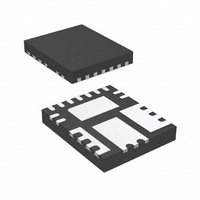
IR3842MTR1PBF International Rectifier, IR3842MTR1PBF Datasheet - Page 21

IR3842MTR1PBF
Manufacturer Part Number
IR3842MTR1PBF
Description
IC REG SYNC SUPIRBUCK 4A 5X6QFN
Manufacturer
International Rectifier
Series
SupIRBuck™r
Type
Step-Down (Buck)r
Datasheet
1.IR3842MTR1PBF.pdf
(32 pages)
Specifications of IR3842MTR1PBF
Internal Switch(s)
Yes
Synchronous Rectifier
Yes
Number Of Outputs
1
Voltage - Output
0.7 ~ 14.4 V
Current - Output
4A
Frequency - Switching
250kHz ~ 1.5MHz
Voltage - Input
1.5 ~ 16 V
Operating Temperature
-40°C ~ 125°C
Mounting Type
Surface Mount
Package / Case
15-PowerVQFN
Power - Output
800mW
Primary Input Voltage
16V
No. Of Outputs
1
Output Voltage
14.4V
Output Current
4A
No. Of Pins
15
Operating Temperature Range
-40°C To +125°C
Msl
MSL 3 - 168 Hours
Filter Terminals
SMD
Rohs Compliant
Yes
Part Status
Active
Package
PQFN / 5 x 6
Circuit
Single Output
Iout (a)
4
Switch Freq (khz)
250 - 1500
Input Range (v)
1.5 - 16
Output Range (v)
0.7 - 0.9*Vin
Ocp Otp Uvlo Pre-bias Soft Start And
PGOOD + EN + SEQ
Server Storage
Yes
Routers Switches
Yes
Base Station Telecom
Yes
Lead Free Status / RoHS Status
Lead free / RoHS Compliant
Other names
IR3842MTR1PBFTR
Based on the frequency of the zero generated by
the output capacitor and its ESR, relative to
crossover frequency, the compensation type can
be different. The table below shows the
compensation
crossover frequency.
F
o
06/18/09
F
F
F
F
F
The compensation network has three poles and
two zeros and they are expressed as follows:
Cross over frequency is expressed as:
H(s) dB
=
P
P
P
Z
Z
1
Fig.15. Type III Compensation network and
its asymptotic gain plot
1
2
3
2
R
=
=
=
=
=
3
0
*
2
2
2
2
Z
C
π
..........
π
π
π
IN
7
Gain(dB)
*
*
*
*
*
R
R
C
R
R
1
C
V
1
3
V
10
10
3
7
osc
7
..........
⎛
⎜
⎜
⎝
in
*
( *
F
1
C
*
C
C
1
types
V
Z
C
R
*
4
1
4
4
OUT
2
7
8
+
*
..........
π
R
R
..........
+
C
..........
C
*
8
9
3
R
3
L
F
10
1
⎞
⎟
⎟
⎠
o
Z
V
2
and
..........
≅
)
*
Fb
REF
..........
..........
C
≅
2
o
π
2
..........
π
*
..........
location
R
R
*
..........
1
E/A
..........
C
F
3
3
1
P
*
7
..........
2
C
*
..........
C
3
R
..........
..........
3
..........
8
..........
..........
F
of
C
P
.....(29)
3
.......(27
Comp
4
......(26)
.....
Frequency
..
(30)
the
(31)
(28)
Z
Ve
f
)
The
potentially faster the load transient response.
However, the crossover frequency should be low
enough to allow attenuation of switching noise.
Typically, the control loop bandwidth or crossover
frequency is selected such that
The DC gain should be large enough to provide
high DC-regulation accuracy. The phase margin
should be greater than 45
For this design we have:
V
V
V
V
L
C
It must be noted here that the value of the
capacitance used in the compensator design
must be the small signal value. For instance, the
small signal capacitance of the 22uF capacitor
used in this design is 12uF at 1.8 V DC bias and
600 kHz frequency. It is this value that must be
used
compensation. The small signal value may be
obtained from the manufacturer’s datasheets,
design tools or SPICE models. Alternatively, they
may also be inferred from measuring the power
stage transfer function of the converter and
measuring the double pole frequency F
using equation (16) to compute the small signal
C
These result to:
F
F
F
Select crossover frequency: F
Since F
place the pole and zeros.
o
LC
ESR
s
in
o
osc
ref
o
o
=1.5 uH
=1.8V
/2=300 kHz
=4x22uF, ESR=3mOhm each
.
=12V
=0.7V
=18.76 kHz
=1.8V
Compensator
Compensator
Type
Type
=4.4 MHz
higher
Type III
Type III
for
Type II
Type II
LC
<F
all
o
<F
F
o
the
s
≤
computations
/2<F
(
1/5
F
F
LC
LC
crossover
F
F
IR3842MPbF
~
ESR
<F
<F
F
F
LC
LC
1/10
ESR
ESR
<F
<F
ESR
ESR
, TypeIII is selected to
o
o
o
)
for overall stability.
vs F
vs F
<F
<F
<F
<F
*
F
o
o
o
ESR
ESR
s
<F
<F
=100 kHz
o
o
related
s
s
frequency,
/2
/2
Electrolytic
Electrolytic
Tantalum
Tantalum
Output
Output
Capacitor
Capacitor
Tantalum
Tantalum
Ceramic
Ceramic
to
LC
21
and
the
the


