MC34163PG ON Semiconductor, MC34163PG Datasheet
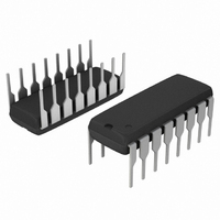
IC REG SW INV DC-DC 3.4A 16DIP

MC34163PG

Manufacturer Part Number
MC34163PG
Description
IC REG SW INV DC-DC 3.4A 16DIP
Manufacturer
ON Semiconductor
Type
Step-Down (Buck), Step-Up (Boost), Invertingr
Datasheet

Specifications of MC34163PG

Internal Switch(s)
Yes
Synchronous Rectifier
No
Number Of Outputs
1
Voltage - Output
1.25 ~ 40 V
Current - Output
3.4A
Frequency - Switching
50kHz
Voltage - Input
2.5 ~ 40 V
Operating Temperature
0°C ~ 70°C
Mounting Type
Through Hole
Package / Case
16-DIP (0.300", 7.62mm)
Output Voltage
1 V to 40 V
Output Current
3 A
Input Voltage
2.5 V to 40 V
Switching Frequency
55 KHz
Operating Temperature Range
0 C to + 70 C
Mounting Style
Through Hole
Lead Free Status / RoHS Status
Lead free / RoHS Compliant
Power - Output
-
Lead Free Status / Rohs Status
Lead free / RoHS Compliant
Other names
MC34163PGOS

Available stocks

Company
Part Number
Manufacturer
Quantity
Price
Part Number:
MC34163PG
Manufacturer:
ON Semiconductor
Quantity:
2
Part Number:
MC34163PG
Manufacturer:
ON/安森美
Quantity:
20 000
MC34163, MC33163
3.4 A, Step-Up/Down/
Inverting Switching
Regulators
contain the primary functions required for dc−to−dc converters. This
series is specifically designed to be incorporated in step−up,
step−down, and voltage−inverting applications with a minimum
number of external components.
comparators, temperature compensated reference, controlled duty
cycle oscillator, driver with bootstrap capability for increased
efficiency, and a high current output switch. Protective features consist
of cycle−by−cycle current limiting, and internal thermal shutdown.
Also included is a low voltage indicator output designed to interface
with microprocessor based systems.
package for improved thermal conduction.
Features
© Semiconductor Components Industries, LLC, 2008
August, 2008 − Rev. 6
Feedback 1
Feedback 2
LVI Output
The MC34163 series are monolithic power switching regulators that
These devices consist of two high gain voltage feedback
These devices are contained in a 16 pin dual−in−line heat tab plastic
GND
I
Capacitor
Output Switch Current in Excess of 3.0 A
Operation from 2.5 V to 40 V Input
Low Standby Current
Precision 2% Reference
Controlled Duty Cycle Oscillator
Driver with Bootstrap Capability for Increased Efficiency
Cycle−by−Cycle Current Limiting
Internal Thermal Shutdown Protection
Low Voltage Indicator Output for Direct Microprocessor Interface
Heat Tab Power Package
Moisture Sensitivity Level (MSL) Equals 1
Pb−Free Packages are Available*
pk
Voltage
Voltage
Timing
Sense
V
CC
8
7
6
5
4
3
2
1
Figure 1. Representative Block Diagram
This device contains 114 active transistors.
LVI
+
+
-
OSC
Control Logic
and Thermal
+
Shutdown
-
+
+
+
-
VFB
(Bottom View)
I
Limit
+
+
10
11
12
13
14
15
16
9
Driver
Collector
Bootstrap
Input
Switch
Collector
GND
Switch
Emitter
1
16
See detailed ordering and shipping information in the package
dimensions section on page 2 of this data sheet.
*For additional information on our Pb−Free strategy
16
and soldering details, please download the
ON Semiconductor Soldering and Mounting
Techniques Reference Manual, SOLDERRM/D.
Voltage Feedback 2
Voltage Feedback 1
Timing Capacitor
1
1
LVI Output
I
ORDERING INFORMATION
pk
GND
Sense
PIN CONNECTIONS
V
x
A
WL = Wafer Lot
YY = Year
WW = Work Week
G
http://onsemi.com
CC
CASE 648C
DW SUFFIX
CASE 751G
SOIC−16W
P SUFFIX
PDIP−16
= 3 or 4
= Assembly Location
= Pb−Free Package
1
2
3
4
5
6
7
8
(Top View)
Publication Order Number:
16
1
16
16
15
14
13
12
11
10
1
9
DIAGRAMS
MARKING
AWLYYWWG
Bootstrap Input
Driver Collector
AWLYYWWG
MC3x163DW
MC3x163P
Switch
Emitter
GND
Switch Collector
MC34163/D

Related parts for MC34163PG

MC34163PG Summary of contents

Page 1

... LVI Output Voltage Feedback Switch Emitter Voltage Feedback GND GND 5 12 Timing Capacitor 6 11 Switch Collector Sense 8 9 Driver Collector pk (Top View) ORDERING INFORMATION and soldering details, please download the ON Semiconductor Soldering and Mounting Techniques Reference Manual, SOLDERRM/D. Publication Order Number: MC34163/D ...

Page 2

... ORDERING INFORMATION Device MC33163DW MC33163DWG MC33163DWR2 MC33163DWR2G MC33163P MC33163PG MC34163DW MC34163DWG MC34163DWR2 MC34163DWR2G MC34163P MC34163PG †For information on tape and reel specifications, including part orientation and tape sizes, please refer to our Tape and Reel Packaging Specifications Brochure, BRD8011/D. Symbol C(switch) V E(switch) V CE(switch) I ...

Page 3

ELECTRICAL CHARACTERISTICS the operating ambient temperature range that applies (Note 5), unless otherwise noted.) Characteristic OSCILLATOR Frequency T = 25°C A Total Variation over and Temperature CC Charge Current Discharge Current Charge to ...

Page 4

25° ∞ off DT ...

Page 5

Darlington Configuration V CC Emitter Sourcing Current to GND - 0.4 Pins Pins GND T = 25°C, (Note 0.8 Bootstrapped, Pin ...

Page 6

V , SUPPLY VOLTAGE (V) CC Figure 14. Standby Supply Current versus Supply Voltage 3 620 pF T Pins 7 Pins GND 2.6 Pin ...

Page 7

Sense + + Timing Capacitor 6 Oscillator C T Shutdown Thermal GND 4 Voltage Feedback Voltage Feedback ...

Page 8

INTRODUCTION The MC34163 series are monolithic power switching regulators optimized for dc−to−dc converter applications. The combination of features in this series enables the system designer to directly implement step−up, step−down, and voltage−inverting converters with a minimum number of external components. ...

Page 9

The switch current is converted to a voltage by inserting a fractional ohm resistor series with V SC switch transistor Q . The voltage drop across R 2 monitored by the Current Sense comparator. If the voltage ...

Page 10

0.075 330 6 Oscillator C T 680 pF 5 Thermal LVI 1. ...

Page 11

0.075 330 6 Oscillator C T 680 pF 5 Thermal Low Voltage + Indicator Output R ...

Page 12

Current 0.25 V Limit 0.075 330 6 Oscillator C T 470 pF 5 Thermal 1.25 V ...

Page 13

Bottom View + + Bottom View + + Bottom View All printed circuit boards are 2.58” in width by 1.9” in height. Figure 27. Printed Circuit Board and Component Layout + + ...

Page 14

Calculation Step−Down V out ) off (Notes sat * V out off ƒ off 32.143 · ...

Page 15

16X 0.005 (0.13) PACKAGE DIMENSIONS PDIP−16 P SUFFIX CASE 648C−04 ISSUE SEATING PLANE http://onsemi.com 15 NOTES: 1. DIMENSIONING AND TOLERANCING PER ASME Y14.5M, 1994. ...

Page 16

... Opportunity/Affirmative Action Employer. This literature is subject to all applicable copyright laws and is not for resale in any manner. PUBLICATION ORDERING INFORMATION LITERATURE FULFILLMENT: Literature Distribution Center for ON Semiconductor P.O. Box 5163, Denver, Colorado 80217 USA Phone: 303−675−2175 or 800−344−3860 Toll Free USA/Canada Fax: 303− ...

Related keywords