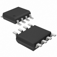
MAX629ESA+ Maxim Integrated Products, MAX629ESA+ Datasheet - Page 8

MAX629ESA+
Manufacturer Part Number
MAX629ESA+
Description
IC DVR MOSFET DUAL NON-INV 8SOIC
Manufacturer
Maxim Integrated Products
Type
Step-Up (Boost), Inverting, Flyback, Sepicr
Datasheet
1.MAX629ESA.pdf
(12 pages)
Specifications of MAX629ESA+
Internal Switch(s)
Yes
Synchronous Rectifier
No
Number Of Outputs
1
Voltage - Output
±28V
Current - Output
500mA
Frequency - Switching
300kHz
Voltage - Input
2.7 ~ 5.5 V
Operating Temperature
-40°C ~ 85°C
Mounting Type
Surface Mount
Package / Case
8-SOIC (3.9mm Width)
Power - Output
471mW
Output Voltage
28 V
Input Voltage
2.7 V to 5.5 V
Supply Current
80 uA
Switching Frequency
300 KHz
Maximum Operating Temperature
+ 85 C
Minimum Operating Temperature
- 40 C
Lead Free Status / RoHS Status
Lead free / RoHS Compliant
28V, Low-Power, High-Voltage,
Boost or Inverting DC-DC Converter
The MAX629’s high switching frequency demands a
high-speed rectifier. Schottky diodes, such as the
1N5819 or MBR0530L, are recommended. Make sure
that the diode’s peak current rating exceeds the peak
current set by ISET, and that its breakdown voltage
exceeds the output voltage. Schottky diodes are pre-
ferred due to their low forward voltage. However, ultra-
high-speed silicon rectifiers are also acceptable. Table
1 lists Schottky diode suppliers.
The primary criterion for selecting the output filter
capacitor is low effective series resistance (ESR). The
product of the peak inductor current and the output fil-
ter capacitor’s ESR determines the amplitude of the
high-frequency ripple seen on the output voltage.
These requirements can be balanced by appropriate
selection of the current limit, as discussed in the S etting
the Current Limit section. Table 1 lists some low-ESR
capacitor suppliers. See the Output Voltage Ripple
graph in the Typical Operating Characteristics section.
Although the output current of many MAX629 applica-
tions may be relatively small, the input must be
designed to withstand current transients equal to the
inductor current limit. The input bypass capacitor
reduces the peak currents drawn from the voltage
Table 1. Component Suppliers
8
CAPACITORS
AVX: TPS series
Matsuo: 267 series
Sprague: 595D series
DIODES
Motorola: MBR0530L
Nihon: EC11 FS1 series
INDUCTORS
Coilcraft: DO1608 and
Murata-Erie: LQH4 series
Sumida: CD43, CD54,
and CDRH62B series
TDK: NLC565050 series
_______________________________________________________________________________________
SUPPLIER
DT1608 series
(803) 946-0690
(714) 969-2491
(603) 224-1961
(602) 303-5454
(805) 867-2555
(847) 639-6400
(814) 237-1431
(847) 956-0666
(847) 390-4373
PHONE
Capacitor Selection
Input Bypass Capacitor
Output Filter Capacitor
Diode Selection
(803) 626-3123
(714) 960-6492
(603) 224-1430
(602) 994-6430
(805) 867-2698
(847) 639-1469
(814) 238-0490
(847) 956-0702
(847) 390-4428
FAX
source, and reduces noise caused by the MAX629’s
switching action. The input source impedance deter-
mines the size of the capacitor required at the input
(V
capacitor is recommended. A 10µF, low-ESR capacitor
is adequate for most applications, although smaller
bypass capacitors may also be acceptable. Bypass the
IC separately with a 0.1µF ceramic capacitor placed as
close as possible to the V
Bypass REF to GND with a 0.1µF ceramic capacitor for
REF currents up to 10µA. REF can source up to 100µA
of current for external loads. For 10µA ≤ I
bypass REF with a 0.47µF capacitor.
Parallel a capacitor (C
feedback loop and ensure stability (Figures 2 and 3).
Values up to 270pF are recommended for most appli-
cations. Choose the lowest capacitor value that
ensures stability; high capacitance values may
degrade line regulation.
Many biasing applications require an adjustable output
voltage, which is easily obtained using the configura-
tion in Figure 4. In this circuit, an external bias voltage
(which may be generated by a potentiometer, a DAC,
or other means) is coupled to FB through the resistor
R
where V
the section Setting the Output Voltage , and V
to either V
0V for the negative configuration. Proper choice of R
provides a wide range of available output voltages
using simple external components to generate V
Although, in many cases, the MAX629 and the inductor
are powered from the same source, it is often advanta-
geous in battery-powered applications to power the
device from an available regulated supply and to
power the inductor directly from a battery. The MAX629
requires a +2.7V to +5.5V supply at V
tor can be powered from as low as +0.8V, significantly
__________Applications Information
B
IN
. The output voltage of this circuit is given by:
). As with the output filter capacitor, a low-ESR
INIT
V
REF
OUT
is the fixed output voltage as calculated in
(1.25V) for the positive configuration or
Adjusting the Output Voltage
V
INIT
F
) across R1 to compensate the
CC
R
R1
B
and GND pins.
Input Voltage Range
Feed-Forward Capacitor
(V
FB
Reference Capacitor
CC
V
BIAS
, but the induc-
REF
)
FB
≤ 100µA,
is equal
BIAS
.
B


