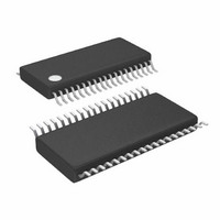
LTC3856EFE#PBF Linear Technology, LTC3856EFE#PBF Datasheet - Page 16

LTC3856EFE#PBF
Manufacturer Part Number
LTC3856EFE#PBF
Description
IC DCDC SWITCH
Manufacturer
Linear Technology
Type
Step-Down (Buck)r
Datasheet
1.LTC3856EFEPBF.pdf
(40 pages)
Specifications of LTC3856EFE#PBF
Internal Switch(s)
No
Synchronous Rectifier
Yes
Number Of Outputs
1
Voltage - Output
0.6 ~ 5 V
Frequency - Switching
250kHz ~ 770kHz
Voltage - Input
4.5 ~ 38 V
Operating Temperature
-40°C ~ 125°C
Mounting Type
Surface Mount
Package / Case
38-TSSOP Exposed Pad, 38-eTSSOP, 38-HTSSOP
Lead Free Status / RoHS Status
Lead free / RoHS Compliant
Current - Output
-
Power - Output
-
LTC3856
applicaTions inForMaTion
Low Value Resistors Current Sensing
A typical sensing circuit using a discrete resistor is shown
in Figure 2a. R
output current. The current comparator has a maximum
threshold, V
The input common mode range of the current compara-
tor is 0V to 5V. The current comparator threshold sets the
peak of the inductor current, yielding a maximum average
output current, I
peak-to-peak ripple current, ∆I
resistor value, use the equation:
Because of possible PCB noise in the current sensing loop,
the AC current sensing ripple of ∆V
also needs to be checked in the design to get a good
signal-to-noise ratio. In general, for a reasonably good
PCB layout, a 10mV ∆V
a conservative number to start with, either for R
DCR sensing applications. For previous generation current
mode controllers, the maximum sense voltage was high
enough (e.g., 75mV for the LTC1628/LTC3728 family)
that the voltage drop across the parasitic inductance of
the sense resistor represented a relatively small error. For
today’s highest current density solutions, however, the
value of the sense resistor can be less than 1mΩ and the
peak sense voltage can be as low as 20mV. In addition,
inductor ripple currents greater than 50% with operation
R
SENSE
20mV/DIV
V
SENSE
=
Figure 3. Voltage Waveform Measured
Directly Across the Sense Resistor
SENSE(MAX)
I
V
(
MAX
SENSE MAX
SENSE
MAX
)
+
, equal to the peak value less half the
(
∆
is chosen based on the required
2
SENSE
, determined by the I
I
L
500ns/DIV
)
voltage is recommended as
L
. To calculate the sense
SENSE
3856 F03
= ∆I
LIM
L
V
ESL(STEP)
• R
SENSE
setting.
SENSE
or
up to 1MHz are becoming more common. Under these
conditions the voltage drop across the sense resistor’s
parasitic inductance is no longer negligible. A typical sens-
ing circuit using a discrete resistor is shown in Figure 2a.
In previous generations of controllers, a small RC filter
placed near the IC was commonly used to reduce the ef-
fects of capacitive and inductive noise coupled in the sense
traces on the PCB. A typical filter consists of two series
10Ω resistors connected to a parallel 1000pF capacitor,
resulting in a time constant of 20ns. This same RC filter,
with minor modifications, can be used to extract the resis-
tive component of the current sense signal in the presence
of parasitic inductance. For example, Figure 3 illustrates
the voltage waveform across a 2mΩ sense resistor with
a 2010 footprint for the 1.2V/15A converter operating at
100% load. The waveform is the superposition of a purely
resistive component and a purely inductive component.
It was measured using two scope probes and waveform
math to obtain a differential measurement. Based on
additional measurements of the inductor ripple current
and the on-time and off-time of the top switch, the value
of the parasitic inductance was determined to be 0.5nH
using the equation:
If the RC time constant is chosen to be close to the
parasitic inductance divided by the sense resistor (L/R),
the resulting waveform looks resistive again, as shown
in Figure 4. For applications using low maximum sense
voltages, check the sense resistor manufacturer’s data
ESL
Figure 4. Voltage Waveform Measured After
the Sense Resistor Filter. C
=
20mV/DIV
V
V
ESL STEP
SENSE
∆
(
I
L
)
t
t
ON
ON
+
•
t
500ns/DIV
t
OFF
OFF
F
= 1000pF , R
3856 F04
F
= 100Ω
3856f
(1)


