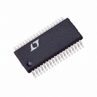
LTC3732CG Linear Technology, LTC3732CG Datasheet - Page 8

LTC3732CG
Manufacturer Part Number
LTC3732CG
Description
IC BUCK SYNC ADJ 5A 36SSOP
Manufacturer
Linear Technology
Type
Step-Down (Buck)r
Datasheet
1.LTC3732CG.pdf
(28 pages)
Specifications of LTC3732CG
Internal Switch(s)
No
Synchronous Rectifier
Yes
Number Of Outputs
1
Voltage - Output
1.1 ~ 7 V
Current - Output
5A
Frequency - Switching
250kHz ~ 600kHz
Voltage - Input
4.5 ~ 32 V
Operating Temperature
0°C ~ 70°C
Mounting Type
Surface Mount
Package / Case
36-SSOP
Lead Free Status / RoHS Status
Contains lead / RoHS non-compliant
Power - Output
-
Available stocks
Company
Part Number
Manufacturer
Quantity
Price
Part Number:
LTC3732CG
Manufacturer:
LT/凌特
Quantity:
20 000
Part Number:
LTC3732CG#PBF
Manufacturer:
LT/凌特
Quantity:
20 000
Company:
Part Number:
LTC3732CG#TR
Manufacturer:
LT
Quantity:
2 500
PI FU CTIO S
LTC3732
VID0 to VID4: Output Voltage Programming Input Pins. A
3 A internal pull-up current is provided on each input pin.
See Table 1 for details. Do not apply voltage to these pins
prior to the application of voltage on the V
PLLIN: Synchronization Input to Phase Detector. This pin
is internally terminated to SGND with 50k . The phase-
locked loop will force the rising top gate signal of control-
ler 1 to be synchronized with the rising edge of the PLLIN
signal.
PLLFLTR: The phase-locked loop’s lowpass filter is tied to
this pin. Alternatively, this pin can be driven with an AC or
DC voltage source to vary the frequency of the internal
oscillator. (Do not apply voltage directly to this pin prior to
the application of voltage on the V
FCB: Forced Continuous Control Input. The voltage ap-
plied to this pin sets the operating mode of the controller.
The forced continuous current mode is active when the
applied voltage is less than 0.6V. Burst Mode operation
will be active when the pin is allowed to float and a stage
shedding mode will be active if the pin is tied to the V
(Do not apply voltage directly to this pin prior to the
application of voltage on the V
IN
amplifier with internal precision resistors. This provides
true remote sensing of both the positive and negative load
terminals for precise output voltage control.
DIFFOUT: Output of the Remote Output Voltage Sensing
Differential Amplifier.
EAIN: This is the input to the error amplifier which com-
pares the VID divided, feedback voltage to the internal
0.6V reference voltage.
PADDLE (UHF Package Only): This pin is connected to
the heat spreading metal pad at the center of the package
bottom and is tied to the IC’s substrate. It must be
connected to the SGND pin.
SGND: Signal Ground. This pin must be routed separately
under the IC to the PGND pin and then to the main ground
plane.
SENSE1
SENSE3
parator. The I
SENSE
the current trip threshold level.
8
+
U
, IN
–
–
+
–
and SENSE
: Inputs to a precision, unity-gain differential
: The Inputs to Each Differential Current Com-
, SENSE2
U
TH
pin voltage and built-in offsets between
+
U
+
, SENSE3
pins, in conjunction with R
CC
+
, SENSE1
pin.)
CC
pin.)
CC
–
, SENSE2
pin.
SENSE
CC
, set
pin.
–
,
RUN/SS: Combination of Soft-Start, Run Control Input
and Short-Circuit Detection Timer. A capacitor to ground
at this pin sets the ramp time to full current output as well
as the time delay prior to an output voltage short-circuit
shutdown. A minimum value of 0.01 F is recommended
on this pin.
I
pensation Point. All three current comparator’s thresholds
increase with this control voltage.
PGND: Driver Power Ground. This pin connects directly to
the sources of the bottom N-channel external MOSFETs
and the (–) terminals of C
BG1 to BG3: High Current Gate Drives for Bottom N-
Channel MOSFETs. Voltage swing at these pins is from
ground to V
V
controller circuit power as well as the high power pulses
supplied to drive the external MOSFET gates, this pin
needs to be very carefully and closely decoupled to the IC’s
PGND pin.
DRV
the bottom MOSFET on-chip drivers. Tie this pin to the V
pin and carefully decouple this pin to the PGND pin with a
minimum of 5 F of ceramic capacitance immediately
adjacent to the IC package.
SW1 to SW3: Switch Node Connections to Inductors.
Voltage swing at these pins is from a Schottky diode
(external) voltage drop below ground to V
the external MOSFET supply rail).
TG1 to TG3: High Current Gate Drives for Top N-channel
MOSFETs. These are the outputs of floating drivers with a
voltage swing equal to the boost voltage source superim-
posed on the switch node voltage SW.
BOOST1 to BOOST3: Positive Supply Pins to the Topside
Floating Drivers. Bootstrapped capacitors, charged with
external Schottky diodes and a boost voltage source, are
connected between the BOOST and SW pins. Voltage
swing at the BOOST pins is from boost source voltage
(typically V
V
PGOOD: This open-drain output is pulled low when the
output voltage has been outside the PGOOD tolerance
window for the V
TH
CC
IN
: Error Amplifier Output and Switching Regulator Com-
: Main Supply Pin. Because this pin supplies both the
is the external MOSFET supply rail).
CC
(UHF Package Only): This pin provides power to
CC
CC
) to this boost source voltage + V
.
PGDLY
delay of approximately 100 s.
IN
.
IN
(where V
IN
(where
IN
3732f
CC
is


