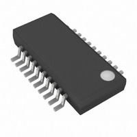
MAX8544EEP+ Maxim Integrated Products, MAX8544EEP+ Datasheet - Page 25

MAX8544EEP+
Manufacturer Part Number
MAX8544EEP+
Description
IC CNTRLR STEP DOWN 20-QSOP
Manufacturer
Maxim Integrated Products
Type
Step-Down (Buck)r
Datasheet
1.MAX8543EEE.pdf
(27 pages)
Specifications of MAX8544EEP+
Internal Switch(s)
No
Synchronous Rectifier
No
Number Of Outputs
1
Voltage - Output
0.8 ~ 11 V
Current - Output
25A
Frequency - Switching
200kHz ~ 1MHz
Voltage - Input
3 ~ 13.2 V
Operating Temperature
-40°C ~ 85°C
Mounting Type
Surface Mount
Package / Case
20-QSOP
Power - Output
727mW
Output Voltage
0.8 V to 11.88 V
Output Current
25000 mA (Max)
Mounting Style
SMD/SMT
Switching Frequency
200 KHz to 1000 KHz
Maximum Operating Temperature
+ 85 C
Minimum Operating Temperature
- 40 C
Synchronous Pin
Yes
Topology
Buck
Lead Free Status / RoHS Status
Lead free / RoHS Compliant
3.43kHz << f
Since f
Select the nearest standard value: C
Select the nearest standard value: C
R3 = R
C8 = C
C7 = C
f
R
C
pMOD
C
C
=
=
=
=
=
=
f
zMOD
C
R
⎛
⎝
2
2
V
2 5
0 8
zMOD
(
C
0 167
C
F
π
π (
V
R
0 167 600 10
G
OUT
LOAD
F
.
.
.
Lossless Sensing, Synchronization, and OVP
×
×
FB
.
Step-Down Controllers with Prebias Startup,
LOAD
= 220kΩ
= 10pF
= 220pF
MOD fc
C
=
=
360 10
×
OUT
2
2
=
(
=
×
×
110 10
(
+
C
< f
π
π (
×
×
( )
2
(
2
g
+
f
×
×
⎛
⎜
⎝
600 10
< 120kHz; select f
S
−
π (
π
C
R
R
mEA
f
6
R
S
LOAD
LOAD
×
220 10
× ×
×
)
:
×
×
×
C
1
=
=
×
L C
______________________________________________________________________________________
×
⎛
⎜
⎜
⎜
⎝
f
C
1
pMOD
360 10
0 167
0 167
L
×
G
4 5
.
.
×
+
OUT
−
3
×
)
×
.
f
f
f
MOD dc
6
×
zMOD
S
S
)( .
1
3
G
OUT
×
×
)
0 8 10
×
+
R
×
120 10
)( .
×
MOD fc
L
L
×
(
(
C
0 8 10
3
600 10
600 10
×
1
+
<<
1
88 4 10
3 43 10
0 175
f
1
) ( .
(
×
ESR
C
ESR
.
.
×
×
×
−
×
×
.
( )
f
6
C
⎞
⎟
⎠
)
88 4 10
)
3
3
−
×
×
×
×
)
)
6
≤
3
×
×
×
−
×
)(
0 005
f
6
⎛
⎝
⎛
⎝
C
f
f
pMOD
( .
zMOD
0 8 10
0 8 10
f
5
88 4 10
360 10
S
.
) (
zMOD
×
.
.
3
3
⎞
⎠
= 120kHz.
×
×
C
F
220 10
=
×
= 10pF:
= 220pF
3
−
−
×
=
0 175
6
6
)
×
⎞
⎠
⎞
⎠
.
88 4
=
+
−
0 005
6
3
8 2
.
.
)
3
)
.
kHz
)
=
pF
⎞
⎟
⎟
⎟
⎠
=
220
=
202
3 43
.
k
kHz
pF
Ω
Careful PC board layout is critical to achieve low
switching losses and clean, stable operation. The
switching power stage requires particular attention.
Follow these guidelines for good PC board layout:
1) Place IC decoupling capacitors as close to IC pins
2) For output current greater than 10A, a four-layer PC
3) Connect input, output, snubber, and VL capacitors
4) Place the inductor current-sense resistor and capaci-
5) Place the MOSFET as close as possible to the IC to
6) Connect the drain leads of the power MOSFET to a
7) Place the feedback and compensation components
Refer to the MAX8544 evaluation kit for an example layout.
as possible. Keep separate the power ground
plane and the signal ground plane. Place the input
ceramic decoupling capacitor directly across and
as close as possible to the high-side MOSFET’s
drain and the low-side MOSFET’s source. This is to
help contain the high switching current within this
small loop.
board is recommended. Pour a signal ground
plane in the second layer underneath the IC to min-
imize noise coupling.
to the power ground plane; connect all other
capacitors to the signal ground plane.
tor as close to the inductor as possible. Make a
Kelvin connection to minimize the effect of PC board
trace resistance. Place the input bias balance resistor
and bypass capacitor (R5 and C10 in Figures 7 and
8) near CS-. Run two closely parallel traces from
across the capacitor (C9 in Figures 7 and 8) to CS+
and CS-. Place the decoupling capacitor C11 close
to CS+ and CS- pins.
minimize trace inductance of the gate-drive loop. If
parallel MOSFETs are used, keep the trace lengths
to both gates equal.
large copper area to help cool the device. Refer to
the power MOSFET data sheet for recommended
copper area.
as close to the IC pins as possible. Connect the
feedback-divider resistor from FB to the output as
close as possible to the farthest output capacitor.
Applications Information
PC Board Layout Guidelines
25


