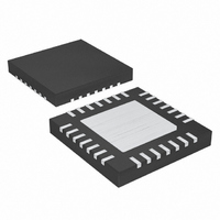
MAX5073ETI+ Maxim Integrated Products, MAX5073ETI+ Datasheet - Page 10

MAX5073ETI+
Manufacturer Part Number
MAX5073ETI+
Description
IC CONV BUCK/BOOST 28-TQFN
Manufacturer
Maxim Integrated Products
Type
Step-Down (Buck), Step-Up (Boost)r
Datasheet
1.MAX5073ETI.pdf
(25 pages)
Specifications of MAX5073ETI+
Internal Switch(s)
Yes
Synchronous Rectifier
No
Number Of Outputs
2
Voltage - Output
0.8 ~ 28 V
Current - Output
1A, 2A
Frequency - Switching
200kHz ~ 2.2MHz
Voltage - Input
4.5 ~ 23 V
Operating Temperature
-40°C ~ 85°C
Mounting Type
Surface Mount
Package / Case
28-TQFN Exposed Pad
Power - Output
2.76W
Lead Free Status / RoHS Status
Lead free / RoHS Compliant
2.2MHz, Dual-Output Buck or Boost Converter
with Internal Power MOSFETs
The MAX5073 converter uses a pulse-width modulation
(PWM) voltage-mode control scheme for each out-of-
phase controller. It is nonsynchronous rectification and
uses an external low-forward-drop Schottky diode for
rectification. The controller generates the clock signal
by dividing down the internal oscillator or the SYNC
input when driven by an external clock, so each con-
troller’s switching frequency equals half the oscillator
frequency (f
tance error amplifier produces an integrated error volt-
age at the COMP pin, providing high DC accuracy. The
voltage at COMP sets the duty cycle using a PWM
comparator and a ramp generator. At each rising edge
of the clock, converter 1’s high-side n-channel MOSFET
turns on and remains on until either the appropriate or
maximum duty cycle is reached, or the maximum cur-
rent limit for the switch is detected. Converter 2 oper-
ates out-of-phase, so the second high-side MOSFET
turns on at each falling edge of the clock.
In the case of buck operation (Figure 1), during each
high-side MOSFET’s on-time, the associated inductor cur-
Figure 1. MAX5073 Dual Buck Regulator Application Circuit
10
______________________________________________________________________________________
OUTPUT2
2.5V/1A
V
IN
= 5.5V TO 23V
SGND
SW
INPUT
= f
OSC
VL
Detailed Description
PGND
/ 2). An internal transconduc-
OFF
ON
CLOCK
OUT
PWM Controller
1
2
3
4
5
6
7
CLKOUT
BST2/VDD2
DRAIN2
DRAIN2
EN2
FB2
COMP2
SYSTEM
CLOCK
28
8
27
9
EP
10
26
MAX5073
11
25
SGND
12
24
rent ramps up. During the second half of the switching
cycle, the high-side MOSFET turns off and forward biases
the Schottky rectifier. During this time, the SOURCE volt-
age is clamped to 0.4V (V
releases the stored energy as its current ramps down,
and provides current to the output. The bootstrap capaci-
tor is also recharged from the inductance energy when
the MOSFET turns off. The circuit goes in discontinuous
conduction mode operation at light load, when the induc-
tor current completely discharges before the next cycle
commences. Under overload conditions, when the induc-
tor current exceeds the peak current limit of the respec-
tive switch, the high-side MOSFET turns off quickly and
waits until the next clock cycle.
In the case of boost operation, the MOSFET is a low-
side switch (Figure 8). During each on-time, the induc-
tor current ramps up. During the second half of the
switching cycle, the low-side switch turns off and for-
ward biases the Schottky diode. During this time, the
DRAIN voltage is clamped to 0.4V (V
and the inductor provides energy to the output as well
as replenishes the output capacitor charge.
13
23
BST1/VDD1
14
22
PGOOD1
DRAIN1
DRAIN1
COMP1
*CONNECT PGND AND SGND TOGETHER AT ONE POINT NEAR THE
EN1
FB1
RETURN TERMINALS OF THE V+ AND VL BYPASS CAPACITORS.
PGOOD2
21
20
19
18
17
16
15
D
ON
) below ground. The inductor
OFF
VL
INPUT
D
) above V
OUTPUT1
3.3V/2A
OUT_


