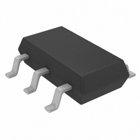
LTC3803ES6-5#TRM Linear Technology, LTC3803ES6-5#TRM Datasheet - Page 7

LTC3803ES6-5#TRM
Manufacturer Part Number
LTC3803ES6-5#TRM
Description
IC FLYBACK SYNC ADJ 1A TSOT23-6
Manufacturer
Linear Technology
Type
Flybackr
Datasheet
1.LTC3803ES6-5TRPBF.pdf
(16 pages)
Specifications of LTC3803ES6-5#TRM
Internal Switch(s)
No
Synchronous Rectifier
No
Number Of Outputs
1
Voltage - Output
Adjustable
Current - Output
1A
Frequency - Switching
200kHz
Voltage - Input
Adjustable
Operating Temperature
-40°C ~ 125°C
Mounting Type
Surface Mount
Package / Case
TSOT-23-6, TSOT-6
Lead Free Status / RoHS Status
Contains lead / RoHS non-compliant
Power - Output
-
Other names
LTC3803ES6-5#TRMTR
Available stocks
Company
Part Number
Manufacturer
Quantity
Price
OPERATION
The LTC3803-5 is a constant frequency current mode
controller for fl yback, SEPIC and DC/DC boost converter
applications in a tiny ThinSOT package. The LTC3803-5 is
designed so that none of its pins need to come in contact
with the input or output voltages of the power supply circuit
of which it is a part, allowing the conversion of voltages well
beyond the LTC3803-5’s absolute maximum ratings.
Main Control Loop
Due to space limitations, the basics of current mode DC/DC
conversion will not be discussed here; instead, the reader
is referred to the detailed treatment in Application Note
19, or in texts such as Abraham Pressman’s Switching
Power Supply Design.
Please refer to the Block Diagram and the Typical Ap-
plication on the front page of this data sheet. An external
resistive voltage divider presents a fraction of the output
voltage to the V
that when the output is at the desired voltage, the V
voltage will equal the 800mV from the internal reference.
If the load current increases, the output voltage will de-
crease slightly, causing the V
800mV. The error amplifi er responds by feeding current
into the I
V
will sink current away from the I
The voltage at the I
modulator formed by the oscillator, current comparator
and RS latch. Specifi cally, the voltage at the I
sets the current comparator’s trip threshold. The current
comparator monitors the voltage across a current sense
resistor in series with the source terminal of the external
MOSFET. The LTC3803-5 turns on the external power
MOSFET when the internal free-running 200kHz oscillator
sets the RS latch. It turns off the MOSFET when the cur-
rent comparator resets the latch or when 80% duty cycle
is reached, whichever happens fi rst. In this way, the peak
current levels through the fl yback transformer’s primary
and secondary are controlled by the I
Since the I
fi er whenever the output voltage is below nominal, and
decreased whenever output voltage exceeds nominal, the
FB
voltage will rise above 800mV and the error amplifi er
TH
TH
/RUN pin. If the load current decreases, the
/RUN voltage is increased by the error ampli-
FB
TH
pin. The divider must be designed so
/RUN pin commands the pulse-width
FB
pin voltage to fall below
TH
/RUN pin.
TH
/RUN voltage.
TH
/RUN pin
FB
pin
voltage regulation loop is closed. For example, whenever
the load current increases, output voltage will decrease
slightly, and sensing this, the error amplifi er raises the
I
raising the current comparator threshold, thus increasing
the peak currents through the transformer primary and
secondary. This delivers more current to the load, bringing
the output voltage back up.
The I
the control loop. Typically, an external series RC network
is connected from I
optimal response to load and line transients. The impedance
of this RC network converts the output current of the error
amplifi er to the I
comparator threshold and commands considerable infl u-
ence over the dynamics of the voltage regulation loop.
Start-Up/Shutdown
The LTC3803-5 has two shutdown mechanisms to disable
and enable operation: an undervoltage lockout on the V
supply pin voltage, and a forced shutdown whenever ex-
ternal circuitry drives the I
transitions into and out of shutdown according to the state
diagram (Figure 1).
TH
(NOMINALLY 4V)
V
CC
/RUN voltage by sourcing current into the I
< V
TH
TURNOFF
/RUN pin serves as the compensation point for
Figure 1. Start-Up/Shutdown State Diagram
TH
/RUN voltage which sets the current
TH
/RUN to ground and is chosen for
SHUT DOWN
LTC3803-5
LTC3803-5
ENABLED
TH
V
(NOMINALLY 0.28V)
/RUN pin low. The LTC3803-5
ITH/RUN
38035 F01
< V
ITHSHDN
LTC3803-5
V
AND V
(NOMINALLY 4.8V)
ITH/RUN
TH
CC
/RUN pin,
> V
> V
ITHSHDN
TURNON
38035fd
7
CC


