LTC3204BEDC-3.3#TRM Linear Technology, LTC3204BEDC-3.3#TRM Datasheet
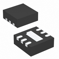
IC SW CAP/DBLR 3.3V 50MA 6DFN

LTC3204BEDC-3.3#TRM

Manufacturer Part Number
LTC3204BEDC-3.3#TRM
Description
IC SW CAP/DBLR 3.3V 50MA 6DFN
Manufacturer
Linear Technology
Type
Switched Capacitor (Charge Pump), Doublerr
Datasheet

Specifications of LTC3204BEDC-3.3#TRM

Internal Switch(s)
Yes
Synchronous Rectifier
No
Number Of Outputs
1
Voltage - Output
3.3V
Current - Output
50mA
Frequency - Switching
1.2MHz
Voltage - Input
1.8 ~ 4.5 V
Operating Temperature
-40°C ~ 85°C
Mounting Type
Surface Mount
Package / Case
6-DFN
Operating Supply Voltage (min)
1.8V
Operating Supply Voltage (max)
4.5V
Operating Temp Range
-40C to 85C
Operating Temperature Classification
Industrial
Pin Count
6
Mounting
Surface Mount
Lead Free Status / RoHS Status
Contains lead / RoHS non-compliant
Power - Output
-
Lead Free Status / Rohs Status
Not Compliant
Other names
LTC3204BEDC-3.3

Available stocks

Company
Part Number
Manufacturer
Quantity
Price
Company:
Part Number:
LTC3204BEDC-3.3#TRMLTC3204BEDC-3.3
Manufacturer:
LT
Quantity:
10 000
Company:
Part Number:
LTC3204BEDC-3.3#TRMLTC3204BEDC-3.3
Manufacturer:
LT/凌特
Quantity:
20 000
FEATURES
APPLICATIO S
TYPICAL APPLICATIO
Fixed 3.3V or 5V Outputs
V
Output Current:
Automatic Burst Mode
(LTC3204-3.3/LTC3204-5)
Constant Frequency Operation at All Loads
(LTC3204B-3.3/LTC3204B-5)
Low Noise Constant Frequency (1.2MHz) Operation*
Built-In Soft-Start Reduces Inrush Current
Shutdown Disconnects Load from Input
Shutdown Current <1µA
Short-Circuit/Thermal Protection
Available in Low Profile 6-Lead DFN Package
2 AA Cell to 3.3V
Li-Ion to 5V
USB On-The-Go Devices
White LED Drivers
Handheld Devices
IN
1.8V to 4.5V (LTC3204-3.3/LTC3204B-3.3)
2.7V to 5.5V (LTC3204-5/LTC3204B-5)
Up to 150mA (LTC3204-5/LTC3204B-5)
Up to 50mA (LTC3204-3.3/LTC3204B-3.3)
Range:
2.7V TO 5.5V
2.2µF
OFF ON
U
1, 7
2
6
®
V
GND
SHDN
IN
LTC3204B-5
LTC3204-5/
Operation with I
C
5
2.2µF
V
C
OUT
U
+
4
3
3204 TA01a
2.2µF
Q
5V
= 48µA
DESCRIPTIO
The LTC
are low noise, constant frequency (1.2MHz) switched ca-
pacitor voltage doublers. The LTC3204-3.3/LTC3204B-3.3
can produce a regulated output voltage of 3.3V
from a minimum input voltage of 1.8V (2 alkaline cells)
whereas the LTC3204-5/LTC3204B-5 can produce 5V from
a minimum of 2.7V (Li-Ion battery) input.
LTC3204-3.3/LTC3204-5 feature automatic Burst Mode
operation at light loads to maintain low supply current
whereas LTC3204B-3.3/LTC3204B-5 feature constant
frequency operation at any load. Built-in soft-start circuitry
prevents excessive inrush current during start-up. Thermal
shutdown and current-limit circuitry allow the parts to
survive a continuous short-circuit from V
High switching frequency minimizes overall solution
footprint by allowing the use of tiny ceramic capaci-
tors. In shutdown, the load is disconnected from the
input and the quiescent current is reduced to <1µA. The
LTC3204-3.3/LTC3204-5/LTC3204B-3.3/LTC3204B-5 are
available in a low profile (0.75mm) 6-lead 2mm × 2mm
DFN package.
All other trademarks are the property of their respective owners.
Burst Mode is a registered trademark of Linear Technology Corporation.
*Protected by U.S. Patents including 6411531.
Charge Pump in 2 × 2 DFN
, LTC and LT are registered trademarks of Linear Technology Corporation.
LTC3204B-3.3/LTC3204B-5
LTC3204-3.3/LTC3204-5/
®
3204-3.3/LTC3204-5/LTC3204B-3.3/LTC3204B-5
Low Noise Regulated
30
25
20
15
10
5
0
0
OUTPUT CAPACITANCE = 2.2µF
V
Output Ripple vs Load Current
IN
= 3.6V
LTC3204-5
25
U
OUTPUT CURRENT (mA)
LTC3204B-5
50
75
100
125
3204 TA01b
OUT
150
to GND.
3204fa
1
®

Related parts for LTC3204BEDC-3.3#TRM

LTC3204BEDC-3.3#TRM Summary of contents

Page 1

... LTC3204-3.3/LTC3204-5/LTC3204B-3.3/LTC3204B-5 are available in a low profile (0.75mm) 6-lead 2mm × 2mm DFN package. , LTC and LT are registered trademarks of Linear Technology Corporation. All other trademarks are the property of their respective owners. Burst Mode is a registered trademark of Linear Technology Corporation. *Protected by U.S. Patents including 6411531. ...

Page 2

... Specifications over the –40°C to 85°C operating temperature range are assured by design, characterization and correlation with statistical process controls. Note 3: R ≡ (2V OL FOR ATIO U W ORDER PART NUMBER LTC3204EDC-3.3 LTC3204EDC-5 TOP VIEW LTC3204BEDC-3 SHDN LTC3204BEDC-5 – PART + MARKING LBJV DC PACKAGE LBNK = 125°C, θ = 80°C/W LBVF ...

Page 3

TYPICAL PERFOR 25° 2.2µF unless otherwise specified) A FLY IN OUT Oscillator Frequency vs Supply Voltage 1.50 1.25 1.00 0.75 0.50 0.25 0 1.5 2.0 2.5 3.0 3.5 4.0 ...

Page 4

LTC3204-3.3/LTC3204-5/ LTC3204B-3.3/LTC3204B-5 TYPICAL PERFOR A CE CHARACTERISTICS 25° 2.2µF unless otherwise specified) A FLY IN OUT Load Regulation 3.35 3.30 3. 3. 1.8V IN ...

Page 5

TYPICAL PERFOR A CE CHARACTERISTICS 25° 2.2µF unless otherwise specified) A FLY IN OUT Load Regulation 5.20 5.10 5. 4. 3.6V IN 4.80 V ...

Page 6

LTC3204-3.3/LTC3204-5/ LTC3204B-3.3/LTC3204B CTIO GND (Pin 1, 7): Ground. These pins should be tied to a ground plane for best performance. The exposed pad must be soldered to PCB ground to provide electrical contact and ...

Page 7

OPERATIO U (Refer to the Block Diagram) The LTC3204-3.3/LTC3204-5/LTC3204B-3.3/LTC3204B-5 use a switched capacitor charge pump to boost V regulated output voltage. Regulation is achieved by sensing the output voltage through an internal resistor divider and modulating the charge pump output ...

Page 8

LTC3204-3.3/LTC3204-5/ LTC3204B-3.3/LTC3204B-5 APPLICATIO S I FOR ATIO U U Power Efficiency The power efficiency (η) of the LTC3204-3.3/LTC3204-5/ LTC3204B-3.3/LTC3204B-5 is similar to that of a linear regulator with an effective input voltage of twice the actual input voltage. This occurs ...

Page 9

APPLICATIO S I FOR ATIO U U where f is the oscillator frequency (typically OSC 1.2MHz) and C is the value of output charge storage OUT capacitor. Also, the value and style of the output capacitor can signifi- cantly affect ...

Page 10

LTC3204-3.3/LTC3204-5/ LTC3204B-3.3/LTC3204B-5 APPLICATIO S I FOR ATIO U U Ceramic Capacitors Ceramic capacitors of different materials lose their capaci- tance with higher temperature and voltage at different rates. For example, a capacitor made of X5R or X7R material will retain ...

Page 11

... SHADED AREA IS ONLY A REFERENCE FOR PIN 1 LOCATION ON THE TOP AND BOTTOM OF PACKAGE Information furnished by Linear Technology Corporation is believed to be accurate and reliable. However, no responsibility is assumed for its use. Linear Technology Corporation makes no representation that the interconnection of its circuits as described herein will not infringe on existing patent rights. LTC3204-3.3/LTC3204-5/ LTC3204B-3 ...

Page 12

... TA02 DRIVE LEDS 100Ω 100Ω 100Ω 100Ω 3200-5 TA03 OUT 2.2µF 5V ±4% 32005 TA05 = 3.3V/5V 20µ –3V/–5V 25µ 5V 3.5mA 5.5V 2.5mA, Q LT/LT 0605 • PRINTED IN USA  LINEAR TECHNOLOGY CORPORATION 2004 3204fa ...

Related keywords