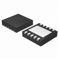
LT1618EDD Linear Technology, LT1618EDD Datasheet - Page 8

LT1618EDD
Manufacturer Part Number
LT1618EDD
Description
IC CONV DC/DC STEPUP CC/CV 10DFN
Manufacturer
Linear Technology
Type
Step-Up (Boost)r
Datasheet
1.LT1618EMSPBF.pdf
(16 pages)
Specifications of LT1618EDD
Internal Switch(s)
Yes
Synchronous Rectifier
No
Number Of Outputs
1
Voltage - Output
1.26 ~ 36 V
Current - Output
1.5A
Frequency - Switching
1.4MHz
Voltage - Input
1.6 ~ 18 V
Operating Temperature
-40°C ~ 85°C
Mounting Type
Surface Mount
Package / Case
10-DFN
Lead Free Status / RoHS Status
Contains lead / RoHS non-compliant
Power - Output
-
Available stocks
Company
Part Number
Manufacturer
Quantity
Price
Company:
Part Number:
LT1618EDD
Manufacturer:
LT
Quantity:
10 000
Part Number:
LT1618EDD
Manufacturer:
LINEAR/凌特
Quantity:
20 000
Company:
Part Number:
LT1618EDD#PBF
Manufacturer:
MAX
Quantity:
34
Part Number:
LT1618EDD#TRPBF
Manufacturer:
LT/凌特
Quantity:
20 000
APPLICATIONS
LT1618
When sensing input current, the sense resistor should be
placed in front of the inductor (between the decoupling
capacitor and the inductor) as shown in the circuits in the
Typical Applications section. This will regulate the average
inductor current and maintain a consistent inductor ripple
current, which will, in turn, maintain a well regulated input
current. Do not place the sense resistor between the input
source and the input decoupling capacitor, as this may
allow the inductor ripple current to vary widely (even
though the average input current and the average inductor
current will still be regulated). Since the inductor current
is a triangular waveform (not a DC waveform like the
output current) some tweaking of the compensation
values (R
a clean inductor ripple current while the constant-current
loop is in effect. For these applications, the constant-
current loop response can usually be improved by reduc-
ing the R
approximately C
compensation network.
Frequency Compensation
The LT1618 has an external compensation pin (V
allows the loop response to be optimized for each applica-
tion. An external resistor and capacitor (or sometimes just
a capacitor) are placed at the V
a zero (or just a pole) to ensure proper loop compensation.
Numerous other poles and zeroes are present in the closed
8
C
C
and C
value, or by adding a capacitor (with a value of
C
C
on the V
/10) in parallel with the R
U
INFORMATION
C
U
pin) may be required to ensure
C
V
pin to provide a pole and
IN
W
L1
C
U
SWITCH
C
NODE
), which
and C
CIRCULATING
Figure 3
C
FREQUENCY
PATH
HIGH
loop transfer function of a switching regulator, so the V
pin pole and zero are positioned to provide the best loop
response. A thorough analysis of the switching regulator
control loop is not within the scope of this data sheet, and
will not be presented here, but values of 2kΩ and 10nF will
be a good choice for many designs. For those wishing to
optimize the compensation, use the 2kΩ and 10nF as a
starting point. For LED backlight applications where a
pulse-width modulation (PWM) signal is used to drive
the I
compensation network. This helps to provide additional
filtering of the PWM signal at the output of the error
amplifier (the V
Switch Node Considerations
To maximize efficiency, switch rise and fall times are made
as short as possible. To prevent radiation and high fre-
quency resonance problems, proper layout of the high
frequency switching path is essential. Keep the output
switch (SW pin), diode and output capacitor as close
together as possible. Minimize the length and area of all
traces connected to the switch pin, and always use a
ground plane under the switching regulator to minimize
interplane coupling. The high speed switching current
path is shown in Figure 3. The signal path including the
switch, output diode and output capacitor contains nano-
second rise and fall times and should be kept as short as
possible.
ADJ
pin, the resistor is usually not included in the
C
LOAD
pin).
1618 • F03
V
OUT
sn1618 1618fas
C


