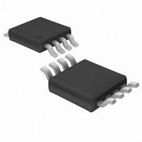
LTC1682CMS8 Linear Technology, LTC1682CMS8 Datasheet - Page 9

LTC1682CMS8
Manufacturer Part Number
LTC1682CMS8
Description
IC MULTI CONFIG ADJ 90MA 8MSOP
Manufacturer
Linear Technology
Type
Step-Up (Boost), Switched Capacitor (Charge Pump), Doublerr
Datasheet
1.LTC1682IS8-5PBF.pdf
(12 pages)
Specifications of LTC1682CMS8
Internal Switch(s)
Yes
Synchronous Rectifier
No
Number Of Outputs
1
Voltage - Output
2.5 ~ 5.5 V
Current - Output
90mA
Frequency - Switching
550kHz
Voltage - Input
1.8 ~ 4.4 V
Operating Temperature
0°C ~ 70°C
Mounting Type
Surface Mount
Package / Case
8-MSOP, Micro8™, 8-uMAX, 8-uSOP,
Lead Free Status / RoHS Status
Contains lead / RoHS non-compliant
Power - Output
-
Available stocks
Company
Part Number
Manufacturer
Quantity
Price
Company:
Part Number:
LTC1682CMS8
Manufacturer:
LT
Quantity:
5 321
Company:
Part Number:
LTC1682CMS8
Manufacturer:
LT
Quantity:
6 980
Company:
Part Number:
LTC1682CMS8
Manufacturer:
microsemi
Quantity:
7 000
Part Number:
LTC1682CMS8
Manufacturer:
LINEAR/凌特
Quantity:
20 000
Part Number:
LTC1682CMS8#PBF
Manufacturer:
LT/凌特
Quantity:
20 000
Company:
Part Number:
LTC1682CMS8#TR
Manufacturer:
MAX
Quantity:
17
Part Number:
LTC1682CMS8#TRPBF
Manufacturer:
LT/凌特
Quantity:
20 000
Company:
Part Number:
LTC1682CMS8-3.3
Manufacturer:
LT
Quantity:
10 000
Part Number:
LTC1682CMS8-3.3
Manufacturer:
LT/凌特
Quantity:
20 000
Part Number:
LTC1682CMS8-3.3#PBF
Manufacturer:
LINEAR/凌特
Quantity:
20 000
The following formula can be used to find the maximum
output voltage that may be programmed for a given
minimum input voltage and output current load:
with the condition that (I
Example:
V
I
R
Max unloaded CPO voltage = 6V
Loaded CPO voltage = 6V – (10mA)(20 ) = 5.8V
V
V
For minimum noise applications, the LDO must be kept out
of dropout to prevent CPO noise from coupling into V
External CPO Loading
The CPO output can drive an external load (an LDO, for
example). The current required by this additional load will
reduce the available current from V
requires 5mA, then the maximum available current at V
will be reduced by 5mA.
Short-Circuit and Thermal Protection
V
cuitry will limit the output current. If the junction tempera-
ture exceeds 150 C, the part will shut down. Excessive
power dissipation due to heavy loads will also cause the
part to shut down when the junction temperature exceeds
150 C. The part will become enabled when the junction
temperature drops below 140 C. If the fault condition
remains in place, the part will cycle between the shutdown
and enabled states.
Capacitor Selection
For best performance it is recommended that low ESR
capacitors be used for C2, C3 and C4 in Figure 1 to
reduce noise and ripple. C2 must be 2 F and C3 must
be equal to or greater than C2. C4 is dependent on the
source impedance. The charge pump demands large
APPLICATIONS
OUT
IN(MIN)
DROPOUT(MAX)
OUT
OUT
CPO(MAX)
V
V
OUT(MAX)
OUT(MAX)
= 10mA
< 5.5V and (I
can be shorted to ground indefinitely. Internal cir-
= 3V
= 20
= (2)(V
= (6V) – (0.2V) – (0.08V) = 5.72V
= 0.08V
OUT
U
IN(MIN)
)(R
OUT
INFORMATION
CPO
U
) – (I
)(R
) < 0.55V
CPO
OUT
OUT
) < 0.55V
W
)(R
. If the external load
IN
CPO
, 0.2V < 1.65V.
) – V
IN
.
U
DROPOUT
OUT
OUT
.
LTC1682/LTC1682-3.3/LTC1682-5
instantaneous currents which may induce ripple onto
a common voltage rail. C4 should be 2 F and a spike
reducing resistor of 2.2
V
A low ESR ceramic capacitor is recommended for the
flying capacitor C1 with a value of 0.22 F. At low load or
high V
on CPO which would reflect as lower ripple on V
If a minimum enable time is required, the CPO output filter
capacitor should be at least 2 the V
When the LDO is first enabled, the CPO capacitor will
dump a large amount of charge into the V
the drop in the CPO voltage falls below 1.45(V
will be disabled and the CPO voltage will have to charge up
to 1.75(V
extends the enable time.
A 1nF filter capacitor for the LTC1682-3.3/LTC1682-5
should be connected between the FILT pin and ground for
optimum noise performance.
Output Ripple
The output noise and ripple on CPO includes a spike
component from the charge pump switches and a droop
component which is dependent on the load current and the
value of C3. The charge pump has been carefully designed
to minimize the spike component; however, low ESR
capacitors are essential to reduce the remaining spike
energy effect on the CPO voltage. C3 should be increased
for high load currents to minimize the droop component.
Ripple components on CPO are greatly reduced at V
the LDO; however, C2 should also be a low ESR capacitor
to improve filtering of the CPO noise.
Shutdown
When SHDN pin is pulled low (< 0.4V), the part will be in
shutdown, the supply current will be < 5 A and V
be connected to ground through a 100 switch. In addi-
tion, CPO will be high impedance and disconnected from
V
If shutdown is not required, connect SHDN to V
will continuously enable the part.
IN
IN
.
and the supply.
IN
a smaller capacitor could be used to reduce ripple
IN
) to enable the LDO. The resulting cycling
may be required between
OUT
OUT
filter capacitor.
capacitor. If
IN
), the LDO
IN
OUT
OUT
OUT
which
.
9
will
by


