LTC1502CMS8-3.3#PBF Linear Technology, LTC1502CMS8-3.3#PBF Datasheet
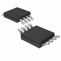
IC DC/DC CONV 3.3V CHRGPMP 8MSOP

LTC1502CMS8-3.3#PBF

Manufacturer Part Number
LTC1502CMS8-3.3#PBF
Description
IC DC/DC CONV 3.3V CHRGPMP 8MSOP
Manufacturer
Linear Technology
Type
Switched Capacitor (Charge Pump)r
Datasheet

Specifications of LTC1502CMS8-3.3#PBF

Internal Switch(s)
Yes
Synchronous Rectifier
No
Number Of Outputs
1
Voltage - Output
3.3V
Current - Output
10mA
Frequency - Switching
500kHz
Voltage - Input
0.9 ~ 1.8 V
Operating Temperature
0°C ~ 70°C
Mounting Type
Surface Mount
Package / Case
8-MSOP, Micro8™, 8-uMAX, 8-uSOP,
Output Voltage
3.3V
Output Current
10mA
Operating Supply Voltage (min)
0.9V
Operating Supply Voltage (max)
1.8V
Operating Temp Range
0C to 70C
Operating Temperature Classification
Commercial
Package Type
MSOP
Pin Count
8
Mounting
Surface Mount
Lead Free Status / RoHS Status
Lead free / RoHS Compliant
Power - Output
-
Lead Free Status / Rohs Status
Compliant

Available stocks

Company
Part Number
Manufacturer
Quantity
Price
Company:
Part Number:
LTC1502CMS8-3.3#PBFLTC1502CMS8-3.3
Manufacturer:
LT
Quantity:
10 000
FEATURES
TYPICAL APPLICATIO
APPLICATIO S
Pagers
Battery Backup Supplies
Portable Electronic Equipment
Handheld Medical Instruments
Glucose Meters
Input Voltage Range: 0.9V to 1.8V
0.9V Guaranteed Start-Up Voltage
Regulated Output Voltage: 3.3V 4%
Output Current: 10mA (V
No Inductors
Shutdown Disconnects Load from V
Low Operating Current: 40 A
Low Shutdown Current: 5 A
Short-Circuit and Overtemperature Protected
Application Circuit Fits in < 0.125in
Available in 8-Pin MSOP and SO Packages
10 F
1 F
Single Cell to 3.3V DC/DC Converter
PCB LAYOUT FITS IN < 0.125IN
1
2
3
4
U
C2
C1
C1
GND
LTC1502-3.3
+
/SHDN
IN
V
C3
C3
OUT
V
IN
+
1V)
8
7
6
5
U
2
1 F
10 F
2
IN
PCB Area
V
SINGLE CELL
NiCd or
ALKALINE
10 F
IN
V
I
OUT
OUT
1502-3.3 TA01
= 10mA
= 3.3V
DESCRIPTIO
The LTC
converter that produces a regulated 3.3V output from a
single alkaline cell input. It requires only five small external
capacitors—no inductors are required. Low supply cur-
rent (40 A typical, 5 A in shutdown) and minimal external
components make the LTC1502-3.3 ideal for space and
power conscious single-cell applications. The total printed
circuit board area of the circuit shown below is less than
0.125in
Forcing the C1
tive pull-down puts the part into shutdown mode. During
shutdown, the internal oscillator is stopped and the load is
disconnected from V
C1
once the pull-down resistance is removed.
The LTC1502-3.3 is short-circuit protected and survives
an indefinite V
available in 8-pin MSOP and SO packages.
, LTC and LT are registered trademarks of Linear Technology Corporation.
/SHDN pin forces the part back into normal operation
Regulated Charge Pump
2
®
.
1502-3.3 is a quadrupler charge pump DC/DC
OUT
/SHDN pin low through an external resis-
3.5
3.4
3.2
3.1
3.0
3.3
short to ground. The LTC1502-3.3 is
U
0.8
IN
DC/DC Converter
Single Cell to 3.3V
T
Output Voltage vs Input Voltage
. An internal pull-up current on the
A
= 25 C
1.0
I
I
INPUT VOLTAGE (V)
OUT
OUT
1.2
= 10mA
= 15mA
LTC1502-3.3
1.4
1.6
1502-3.3 TA02
1.8
1

Related parts for LTC1502CMS8-3.3#PBF

LTC1502CMS8-3.3#PBF Summary of contents

Page 1

... V – C1 /SHDN pin forces the part back into normal operation once the pull-down resistance is removed. The LTC1502-3.3 is short-circuit protected and survives an indefinite V available in 8-pin MSOP and SO packages. , LTC and LT are registered trademarks of Linear Technology Corporation 3.3V OUT I = 10mA OUT 10 F ...

Page 2

... U RATINGS (Note 1) Operating Temperature Range Commercial ............................................ Extended Commercial (Note 4) .......... – Industrial ........................................... – Lead Temperature (Soldering, 10 sec)................. 300 ORDER PART NUMBER C2 1 LTC1502CMS8-3 – C1 /SHDN 3 GND 4 MS8 PART MARKING LTEC 8-LEAD PLASTIC SO T JMAX = 10 F unless otherwise specified. ...

Page 3

W U TYPICAL PERFOR A CE CHARACTERISTICS No Load Input Current vs Input Voltage 0mA OUT – 40 ...

Page 4

LTC1502-3 PIN FUNCTIONS C2 (Pin 1): Charge Pump 1 (CP1) Output. This pin also serves as the input supply for charge pump 2 (CP2). To ensure proper start-up, the C2 pin must not be externally loaded. Bypass ...

Page 5

TEST CIRCUIT SWITCH CLOSED FOR SHUTDOWN U U APPLICATIONS INFORMATION Regulator Operation The LTC1502-3.3 uses a quadrupler charge pump DC/DC converter to produce a boosted output voltage. The quadrupler charge pump consists of two voltage doubler charge pumps (CP1 and ...

Page 6

LTC1502-3 APPLICATIONS INFORMATION LTC1502-3.3 3 – C1 /SHDN 4 GND 100 ON OFF V CTRL Figure 1. Pull-Down Circuitry for Shutdown – will force a logic high on the C1 /SHDN pin and ...

Page 7

... FLASH SHALL NOT EXCEED 0.010" (0.254mm) PER SIDE Information furnished by Linear Technology Corporation is believed to be accurate and reliable. However, no responsibility is assumed for its use. Linear Technology Corporation makes no represen- tation that the interconnection of its circuits as described herein will not infringe on existing patent rights. ...

Page 8

... NiCd OR ALKALINE 1502-3.3 TA03 V = 3.3V OUT I = 300mA OUT (I = 10mA OUT IN BACKUP MODE 100 Q1 2N7002 LOGIC LOW = BACKUP MODE 1502-3.3 TA04 2.5V MSOP Package , 34V, SOT-23 Package OUT Noise 50mA, MSOP OUT 15023f LT/TP 0899 4K • PRINTED IN USA LINEAR TECHNOLOGY CORPORATION 1999 ...

Related keywords