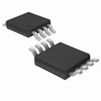
LTC1682CMS8#TR Linear Technology, LTC1682CMS8#TR Datasheet - Page 5

LTC1682CMS8#TR
Manufacturer Part Number
LTC1682CMS8#TR
Description
IC MULTI CONFIG ADJ 90MA 8MSOP
Manufacturer
Linear Technology
Type
Step-Up (Boost), Switched Capacitor (Charge Pump), Doublerr
Datasheet
1.LTC1682IS8-5PBF.pdf
(12 pages)
Specifications of LTC1682CMS8#TR
Internal Switch(s)
Yes
Synchronous Rectifier
No
Number Of Outputs
1
Voltage - Output
2.5 ~ 5.5 V
Current - Output
90mA
Frequency - Switching
550kHz
Voltage - Input
1.8 ~ 4.4 V
Operating Temperature
0°C ~ 70°C
Mounting Type
Surface Mount
Package / Case
8-MSOP, Micro8™, 8-uMAX, 8-uSOP,
Lead Free Status / RoHS Status
Contains lead / RoHS non-compliant
Power - Output
-
Available stocks
Company
Part Number
Manufacturer
Quantity
Price
PIN
TYPICAL PERFOR A CE CHARACTERISTICS
V
should be bypassed with a 2 F low ESR capacitor as
close to the pin as possible for best performance. The V
range is 2.5V to 5.5V.
SHDN (Pin 2): Shutdown Input. A logic low on the SHDN
pin puts the part in shutdown mode. A logic high enables
the part. To continuously enable the part connect SHDN to
V
to ground via a 100
impedance disconnected from V
FB (Pin 3) (LTC1682): The voltage on this pin is compared
to the internal reference voltage (1.235V) by the error
amplifier to keep the output in regulation. An external
resistor divider is required between V
the output voltage.
OUT
IN
U
. When the part is in shutdown, V
(Pin 1): Low Noise Regulated Output Voltage. V
FUNCTIONS
U
5.030
5.020
5.010
5.000
4.990
3.340
3.330
3.320
3.310
3.300
3.290
1.240
1.238
1.236
1.234
–50
U
V
V
I
OUT
OUT
IN
= 3V
–25
= 10mA
switch and CPO will be high
Voltage vs Temperature
W
0
TEMPERATURE ( C)
LTC1682-3.3
LTC1682-5
LTC1682
IN
25
U
.
OUT
OUT
50
will be connected
and FB to adjust
75
100
1682 G09
125
OUT
OUT
LTC1682/LTC1682-3.3/LTC1682-5
FILT (Pin 3) (LTC1682-3.3/LTC1682-5): This pin is used
to filter the internal voltage reference. Typically a 1nF
capacitor is connected from FILT to ground.
GND (Pin 4): System Ground.
C
V
bypassed with a 2 F low ESR capacitor as close to the
pin as possible for best performance. A minimum capaci-
tance value of 0.1 F is required.
C
CPO (Pin 8): Unregulated Charge Pump Output Voltage.
Approximately 1.95(V
low ESR capacitor. If a minimum V
required, the CPO capacitor should be 2 the V
capacitor.
IN
+
–
(Pin 7): Flying Capacitor Positive Input.
(Pin 5): Flying Capacitor Negative Input.
(Pin 6): Input Voltage, 1.8V to 4.4V. V
5.000
4.999
4.998
4.997
4.996
4.995
3.299
3.298
3.297
4.994
4.993
3.300
3.296
3.295
3.294
0
V
OUT
5
Voltage vs Output Current
10
OUTPUT CURRENT (mA)
15
IN
20
) at low loads. Bypass with a 2 F
LTC1682-3.3
25
LTC1682-5
30 35
V
T
40 45 50
IN
A
= 25 C
= 3.3V
1682 G10
OUT
enable time is
IN
should be
5
OUT


