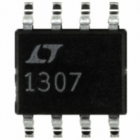
LT1307CS8 Linear Technology, LT1307CS8 Datasheet - Page 9

LT1307CS8
Manufacturer Part Number
LT1307CS8
Description
IC DC/DC CONV SINGLE CELL 8-SOIC
Manufacturer
Linear Technology
Type
Step-Up (Boost)r
Datasheet
1.LT1307CS8PBF.pdf
(20 pages)
Specifications of LT1307CS8
Internal Switch(s)
Yes
Synchronous Rectifier
No
Number Of Outputs
1
Voltage - Output
3.3V, 5V
Current - Output
100mA
Frequency - Switching
600kHz
Voltage - Input
1 ~ 5 V
Operating Temperature
-40°C ~ 85°C
Mounting Type
Surface Mount
Package / Case
8-SOIC (3.9mm Width)
Lead Free Status / RoHS Status
Contains lead / RoHS non-compliant
Power - Output
-
Available stocks
Company
Part Number
Manufacturer
Quantity
Price
Part Number:
LT1307CS8
Manufacturer:
LINEAR/凌特
Quantity:
20 000
Part Number:
LT1307CS8#PBF
Manufacturer:
LINEAR/凌特
Quantity:
20 000
Part Number:
LT1307CS8#TR
Manufacturer:
专营LINEAR
Quantity:
20 000
Part Number:
LT1307CS8#TRPBF
Manufacturer:
LINEAR/凌特
Quantity:
20 000
APPLICATIO S I FOR ATIO
Trace B. Similarly, Figure 4 details the two circuits with a
load step from 5mA to 45mA with a 1.5V input.
The LT1307B also can be used in lower current applica-
tions where a clean, low ripple output is needed. Figure 5
details transient response of a single cell to 3.3V con-
verter, using an inductor value of 100 H. This high induc-
tance minimizes ripple current, allowing the LT1307B to
regulate without skipping cycles. As the load current is
stepped from 5mA to 10mA, the output voltage responds
cleanly. Note that the V
made more conservative (increased C, decreased R).
At light loads, the LT1307B will begin to skip alternate
cycles. The load point at which this occurs can be de-
creased by increasing the inductor value. However, output
ripple will continue to be significantly less than the LT1307
output ripple. Further, the LT1307B can be forced into
micropower mode, where I
pulling down V
DC/DC CONVERTER NOISE CONSIDERATIONS
Switching regulator noise is a significant concern in many
communications systems. The LT1307 is designed to
keep noise energy out of the sensitive 455kHz band at all
load levels while consuming only 60 W to 100 W at no
load. At light load levels, the device is in Burst Mode,
causing low frequency ripple to appear at the output.
Figure 6 details spectral noise directly at the output of
Figure 1’s circuit in a 1kHz to 1MHz bandwidth. The
converter supplies a 5mA load from a 1.25V input. The
Burst Mode fundamental at 5.1kHz and its harmonics are
AC COUPLED
Figure 5. Increasing L to 100 H, Along with R
C
LT1307B Can Be Realized at Light Loads of 5mA to 10mA
100mV/DIV
20mA/DIV
C
I
L
= 20nF and C
10mA
V
5mA
OUT
I
L
V
V
IN
OUT
= 1.25V
= 3.3V
C
to 0.3V or less externally.
OUT
U
= 10 F, Low Noise Performance of
C
pin loop compensation has been
U
1ms/DIV
Q
falls from 1mA to 50 A by
W
C
= 36k,
1307 F05
U
quite evident, as is this particular device’s 575kHz switch-
ing frequency (nominal switching frequency is 600kHz).
Note, however, the absence of significant energy at 455kHz.
Figure 7’s plot reduces the frequency span from 255kHz to
655kHz with a 455kHz center. Burst Mode low frequency
ripple creates sidebands around the 575kHz switching
fundamental. These sidebands have low signal amplitude
at 455kHz, measuring – 55dBmV
further reduced, the Burst Mode frequency decreases.
This spaces the sidebands around the switching fre-
quency closer together, moving spectral energy further
Figure 7. Span Centered at 455kHz Shows – 55dBmV
(1.8 V
Apart Around the Switching Frequency Fundamental of 575kHz
Figure 6. Spectral Noise Plot of 3.3V Converter Delivering
5mA Load. Burst Mode Fundamental at 5.1kHz is 23dBmV
or 14mV
RMS
RMS
) at 455kHz. Burst Mode Creates Sidebands 5.1kHz
–20
–25
–30
–35
–40
–45
–50
–55
–60
–65
–70
–10
–20
–30
–40
–50
–60
40
30
20
10
0
255
1
RBW = 100Hz
RBW = 100Hz
FREQUENCY (kHz)
10
FREQUENCY (kHz)
455
LT1307/LT1307B
100
RMS
. As load current is
1307 F07
1307 F06
1000
655
RMS
RMS
1307fa
9


