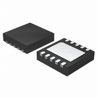
LT3463AEDD Linear Technology, LT3463AEDD Datasheet - Page 2

LT3463AEDD
Manufacturer Part Number
LT3463AEDD
Description
IC CONV DC/DC DUAL MICRPWR 10DFN
Manufacturer
Linear Technology
Type
Invertingr
Datasheet
1.LT3463AEDDPBF.pdf
(8 pages)
Specifications of LT3463AEDD
Internal Switch(s)
Yes
Synchronous Rectifier
No
Number Of Outputs
2
Voltage - Output
1.25 ~ 40 V
Current - Output
250mA
Voltage - Input
2.4 ~ 15 V
Operating Temperature
-40°C ~ 85°C
Mounting Type
Surface Mount
Package / Case
10-DFN
Lead Free Status / RoHS Status
Contains lead / RoHS non-compliant
Power - Output
-
Frequency - Switching
-
Available stocks
Company
Part Number
Manufacturer
Quantity
Price
Company:
Part Number:
LT3463AEDD
Manufacturer:
LT
Quantity:
2 400
Company:
Part Number:
LT3463AEDD
Manufacturer:
LT
Quantity:
10 000
Company:
Part Number:
LT3463AEDD#PBF
Manufacturer:
LT
Quantity:
2 500
Company:
Part Number:
LT3463AEDD#TRPBF
Manufacturer:
LTC
Quantity:
3 874
Company:
Part Number:
LT3463AEDD#TRPBF
Manufacturer:
FUZETEC
Quantity:
7 622
Part Number:
LT3463AEDD#TRPBF
Manufacturer:
LT/凌特
Quantity:
20 000
LT3463/LT3463A
ABSOLUTE AXI U RATI GS
(Note 1)
V
SW1, SW2, V
D2 Voltage ............................................................. –42V
FB1, FB2 Voltage Range .............................. –0.3V to 2V
Junction Temperature ........................................... 125 C
Operating Ambient Temperature Range
Storage Temperature Range ................. – 65 C to 125 C
ELECTRICAL CHARACTERISTICS
temperature range, otherwise specifications are at T
PARAMETER
Minimum Input Voltage
Total Quiescent Current
Shutdown Current
V
V
FB1 Comparator Trip Voltage
FB1 Comparator Hysteresis
FB1 Line Regulation
FB1 Pin Bias Current (Note 3)
FB2 Comparator Trip Voltage
FB2 Comparator Hysteresis
FB2 Line Regulation (V
FB2 Pin Bias Current (Note 4)
SW1 Switch Off Time
SW2 Switch Off Time
Switch V
Switch Current Limit (SW1)
Switch Current Limit (SW2)
Swith Leakage Current (SW1, SW2)
Schottky Forward Voltage (V
Schottky Reverse Leakage Current
SHDN1 Pin Current
SHDN2 Pin Current
SHDN1/SHDN2 Start-Up Threshold
Note 1: Absolute Maximum Ratings are those values beyond which the life
of a device may be impaired.
Note 2: The LT3463/LT3463A are guaranteed to meet performance
specifications from 0 C to 70 C. Specifications over the –40 C to 85 C
2
REF
REF
IN
(Note 2) .............................................. – 40 C to 85 C
, SHDN1, SHDN2 Voltage ................................... 15V
Pin Voltage
Pin Voltage Line Regulation
CESAT
(SW1, SW2)
OUT1
REF
W
Voltage ....................................... 42V
– V
OUT1
FB2
)
, D2)
W W
CONDITIONS
For Both Switchers, Not Switching
V
With 124k to GND
With 124k to GND
High to Low Transition
2.5V < V
V
Low to High Transition
2.5V < V
V
V
V
V
V
I
LT3463
LT3463A
Switch Off, V
I
V
V
V
V
SW
D
SHDN1
FB1
FB2
OUT1
OUT1
FB2
FB2
OUT1
D2
SHDN1
SHDN2
= 150mA
= 150mA
= –42V
= 1.3V
= –0.1V
< 0.1V
= 1V
– V
– V
– V
= V
= 2.5V
= 2.5V
IN
IN
IN
IN
SW
< 15V
< 15V
SHDN2
= 4V
= 0V
SW
= 42V
U
= 42V
A
= 0V
= 25 C. V
The
IN
denotes the specifications which apply over the full operating
= 2.5V, V
PACKAGE/ORDER I FOR ATIO
Consult LTC Marketing for parts specified with wider operating temperature ranges.
operating ambient temperature range are assured by design,
characterization and correlation with statistical process controls.
Note 3: Bias current flows into the FB1 pin.
Note 4: Bias current flows out of the FB2 pin.
V
T
10-LEAD (3mm 3mm) PLASTIC DFN
SHDN
OUT1
SW1
SW2
JMAX
V
D2
IN
AND MUST BE SOLDERED TO PCB
EXPOSED PAD (PIN 11) IS GND
= 125 C,
= 2.5V unless otherwise noted.
1
2
3
4
5
DD PACKAGE
TOP VIEW
JA
11
= 43 C/W,
10
9
8
7
6
JC
= 3 C/W
FB1
SHDN1
SHDN2
V
FB2
REF
1.225
1.23
MIN
180
180
320
0.3
0
U
DD PART MARKING
1.25
0.05
1.25
0.05
0.05
0.01
TYP
300
300
180
250
250
400
750
2.2
0.1
1.5
1.5
40
20
20
8
3
8
1
1
4
4
1
ORDER PART
LT3463EDD
LT3463AEDD
NUMBER
W
LAFC
LBJK
1.275
MAX
1.27
0.10
0.10
0.10
320
320
460
2.4
1.5
60
50
12
50
10
10
1
1
5
5
UNITS
U
3463f
%/V
%/V
%/V
mV
mV
mV
mV
mA
mA
mA
mV
nA
nA
ns
ns
V
A
A
V
V
A
A
A
A
A
V
s
s


