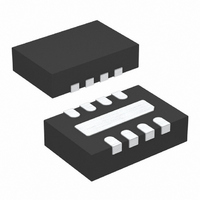
LTC3531EDD-3.3#TRPBF Linear Technology, LTC3531EDD-3.3#TRPBF Datasheet - Page 3

LTC3531EDD-3.3#TRPBF
Manufacturer Part Number
LTC3531EDD-3.3#TRPBF
Description
IC DC/DC CONV 200MA 8-DFN
Manufacturer
Linear Technology
Type
Step-Down (Buck), Step-Up (Boost)r
Datasheet
1.LTC3531EDDPBF.pdf
(16 pages)
Specifications of LTC3531EDD-3.3#TRPBF
Internal Switch(s)
Yes
Synchronous Rectifier
Yes
Number Of Outputs
1
Voltage - Output
3.3V
Current - Output
200mA
Voltage - Input
1.8 ~ 5.5 V
Operating Temperature
-40°C ~ 85°C
Mounting Type
Surface Mount
Package / Case
8-DFN
Lead Free Status / RoHS Status
Lead free / RoHS Compliant
Power - Output
-
Frequency - Switching
-
Available stocks
Company
Part Number
Manufacturer
Quantity
Price
temperature range, otherwise specifi cations are at T
PARAMETER
PMOS D R
PMOS D R
Peak Current Limit
SHDN Input Threshold
SHDN Hysteresis
SHDN Leakage Current
TYPICAL PERFOR
ELECTRICAL CHARACTERISTICS
SHDN
Note 1: Stresses beyond those listed under Absolute Maximum Ratings
may cause permanent damage to the device. Exposure to any Absolute
Maximum Rating condition for extended periods may affect device
reliability and lifetime.
Note 2: This IC includes overtemperature protection that is intended
to protect the device during momentary overload conditions. Junction
temperature will exceed 125°C when overtemperature protection is active.
100
350
300
250
200
150
100
180
160
140
120
60
40
50
80
20
0
0
1.5
1.5
Maximum I
(3.3V Version)
I
IN
L = 10μH
V
DSON
DSON
OUT
Short Circuit vs V
2
2
= 3.3V
(3.3V Version or Adjustable Version set to 3.3V)
(3V Version)
2.5
2.5
OUT
3
3
V
V
vs V
IN
IN
3.5
3.5
(V)
(V)
IN
IN
4
4
W
4.5
4.5
A
5
5
3531 G01
3531 G04
U
5.5
5.5
CE CHARACTERISTICS
300
250
150
100
450
400
350
200
100
50
90
80
70
60
50
40
30
20
10
0
0
1.5
A
1.5
I
V
(3.3V Version)
= 25°C. V
PEAK
L = 10μH
OUT
2
2
, I
Ripple vs C
The
VALLEY
CONDITIONS
V
V
L = 10μH, V
V
2.5
2.5
OUT
OUT
SHDN
●
IN
= 3.1V
= 2.8V
denotes the specifi cations which apply over the full operating
= 3.6V V
3
, I
3
V
V
ZERO
IN
IN
3.5
3.5
I
Continuous operation above the specifi ed maximum operating junction
temperature may result in device degradation or failure.
Note 3: The LTC3531 is guaranteed to meet performance specifi cations
from 0°C to 70°C. Specifi cations over the –40°C to 85°C operating
temperature range are assured by design, characterization and correlation
with statistical process controls.
ZERO
OUT
(V)
IN
(V)
= 5V
10μF
vs V
22μF
I
OUT
4
VALLEY
4
I
IN
PEAK
4.5
4.5
= 3.3V unless otherwise noted.
50mA LOAD
LTC3531-3.3/LTC3531-3
5
5
3531 G02
3531 G05
T
A
5.5
5.5
= 25°C unless otherwise specifi ed.
3.40
3.35
3.30
3.25
3.20
3.15
12
MIN
20
18
16
14
10
295
0.4
0
8
6
4
2
0.1
1.5
Sleep Currents
Load Regulation vs C
(3.3V Version)
V
IN
22μF
= 3.6V
2
TYP
0.01
365
0.8
0.9
60
2.5
1
1
LOAD CURRENT (mA)
3
LTC3531/
V
IN
10μF
MAX
I
3.5
47μF
10
460
VIN
1.4
1
(V)
4
OUT
I
VOUT
100
4.5
5
3531 G03
3521 G06
UNITS
3531fb
3
1000
mA
mV
5.5
μA
Ω
Ω
V


