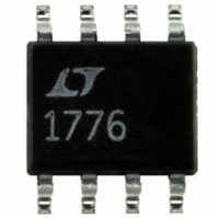
LT1776CS8 Linear Technology, LT1776CS8 Datasheet

LT1776CS8
Specifications of LT1776CS8
Available stocks
Related parts for LT1776CS8
LT1776CS8 Summary of contents
Page 1
... At light loads, rise time is deliberately reduced to avoid pulse skipping behavior. The available SO-8 package and 200kHz switching fre- quency allow for minimal PC board area requirements. , LTC and LT are registered trademarks of Linear Technology Corporation. 100 H* 5V 400mA + 100 F 36 ...
Page 2
... SHDN 12V V 60V 0.5A SW (Note 3) Duty Cycle = INFORMATION ORDER PART TOP VIEW NUMBER LT1776CN8 7 FB LT1776CS8 6 SYNC LT1776IN8 5 V LT1776IS8 IN S8 PACKAGE S8 PART MARKING 8-LEAD PLASTIC SO = 130 C/ W (N8) JA 1776 = 110 C/ W (S8) JA 1776I = MIN TYP MAX 6.7 7.0 7.4 ...
Page 3
ELECTRICAL CHARACTERISTICS The denotes specifications which apply over the full operating temperature range, otherwise specifications are 40V, V open 5V 1.4V unless otherwise noted SYMBOL PARAMETER Timing f Switching ...
Page 4
LT1776 W U TYPICAL PERFORMANCE CHARACTERISTICS Minimum Input Voltage vs Temperature 7.4 7.2 7.0 6.8 6.6 6.4 6.2 6.0 – 100 125 –25 0 TEMPERATURE ( C) 1776 G01 SHDN Pin Shutdown Threshold vs Temperature 900 800 ...
Page 5
W U TYPICAL PERFORMANCE CHARACTERISTICS V Pin Switching Threshold, C Boost Threshold, Clamp Voltage vs Temperature 2.2 2.0 CLAMP VOLTAGE 1.8 1.6 BOOST THRESHOLD 1.4 SWITCHING 1.2 THRESHOLD 1.0 0.8 –50 – 100 125 TEMPERATURE ( ...
Page 6
LT1776 PIN FUNCTIONS 10% and 90% duty cycle. The sync function is internally disabled if the FB pin voltage is low enough to cause oscillator slowdown. If unused, this pin should be grounded. FB (Pin 7): This ...
Page 7
TIMING DIAGRAMS High dV/dt Mode SWDR SWON BOOST SWOFF U OPERATIO The LT1776 is a current mode switching regulator IC that has been optimized for high efficiency operation in high input voltage, ...
Page 8
LT1776 U OPERATIO The system as previously described handles heavy loads (continuous mode) at good efficiency, but it is actually counterproductive for light loads. The method of jam- ming charge into the PNP bases makes it difficult to turn them ...
Page 9
U U APPLICATIONS INFORMATION limits the inductor’s current carrying capability as the I power threatens to overheat the inductor. If applicable, remember to include the condition of output short circuit. Although the peak current rating of the inductor can be ...
Page 10
... SW maximum possible efficiency at light loads. This require- ment can be satisfied by forcing the part into Burst Mode operation. The use of an external comparator whose node. The Burst Mode is a trademark of Linear Technology Corporation and the resulting overdrive further C C and high f ...
Page 11
U U APPLICATIONS INFORMATION output controls the shutdown pin allows high efficiency at light loads through Burst Mode operation behavior (see Typical Applications and Figure 8). Maximum Load/Short-Circuit Considerations The LT1776 is a current mode controller. It uses the V ...
Page 12
LT1776 U U APPLICATIONS INFORMATION However, remember that oscillator slowdown to achieve short-circuit protection (discussed above) is dependent on FB pin behavior, and this in turn, is sensitive to FB node external impedance. Figure 2 shows the typical relation- ship ...
Page 13
U U APPLICATIONS INFORMATION The high speed switching current path is shown schemati- cally in Figure 3. Minimum lead length in these paths is essential to ensure clean switching and minimal EMI. The paths containing the input capacitor, output switch ...
Page 14
LT1776 U TYPICAL APPLICATIONS Minimum Component Count Application Figure 4a shows a basic “minimum component count” application. The circuit produces 500mA I with input voltages in the range of 10V to 40V. The typical P /P ...
Page 15
U TYPICAL APPLICATIONS 158k 1% R5 6.19k 1% chosen to be significantly above the SHDN pin input current to minimize its error contribution, but signifi- cantly below the typical 3.8mA the LT1776 draws in lockout mode. Resistor ...
Page 16
LT1776 U TYPICAL APPLICATIONS V IN 10V TO 40V + C1 C1: PANASONIC HFQ 63V C2: AVX D CASE 100 F 10V TPSD107M010R0080 C3: 2200pF, X7R Burst Mode Operation Configuration Figure 4b demonstrates that power supply efficiency ...
Page 17
U TYPICAL APPLICATIONS R7 10M Q2* 2N2369 NC C1: PANASONIC HFQ 63V C2: AVX D CASE 100 F 10V TPSD107M010R0080 D1: MOTOROLA 100V, 1A, SMD SCHOTTKY MBRS1100 (T3) L1: COILCRAFT DO3316-104 *ANY NPN WITH EMITTER-BASE BREAKDOWN OF ...
Page 18
LT1776 U TYPICAL APPLICATIONS Figure 7b shows that efficiency is typically maintained at 75% or better down to a load current of 10mA. Even at a load of 1mA, efficiency is still a respectable 58% to 68%, depending on V ...
Page 19
... FLASH SHALL NOT EXCEED 0.010" (0.254mm) PER SIDE Information furnished by Linear Technology Corporation is believed to be accurate and reliable. However, no responsibility is assumed for its use. Linear Technology Corporation makes no represen- tation that the interconnection of its circuits as described herein will not infringe on existing patent rights. ...
Page 20
... BATTERY 100 F R2 10V 12.1k 1% C1: PANASONIC HFQ C2: AVX TPSD107M010R0080 L1: COILCRAFT DO3316P-104 1776 TA02 Battery Charger Output Voltage vs Output Current 100 150 OUTPUT CURRENT (mA) 1776 TA04 sn1776 1776fs LT/TP 0499 4K • PRINTED IN LINEAR TECHNOLOGY CORPORATION 1998 200 250 1776 TA05 USA ...


