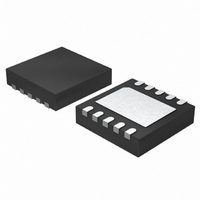
LT3757IDD#TRPBF Linear Technology, LT3757IDD#TRPBF Datasheet - Page 10

LT3757IDD#TRPBF
Manufacturer Part Number
LT3757IDD#TRPBF
Description
IC CTRLR DC/DC ADJ 10-DFN
Manufacturer
Linear Technology
Type
Step-Up (Boost), Inverting, Flyback, Sepicr
Datasheet
1.LT3757EDDPBF.pdf
(36 pages)
Specifications of LT3757IDD#TRPBF
Internal Switch(s)
No
Synchronous Rectifier
No
Number Of Outputs
1
Frequency - Switching
100kHz ~ 1MHz
Voltage - Input
2.9 ~ 40 V
Operating Temperature
-40°C ~ 125°C
Mounting Type
Surface Mount
Package / Case
10-DFN
Lead Free Status / RoHS Status
Lead free / RoHS Compliant
Current - Output
-
Voltage - Output
-
Power - Output
-
Available stocks
Company
Part Number
Manufacturer
Quantity
Price
applicaTions inForMaTion
LT3757
For applications where the SHDN/UVLO pin is only used
as a logic input, the SHDN/UVLO pin can be connected
directly to the input voltage V
INTV
An internal, low dropout (LDO) voltage regulator produces
the 7.2V INTV
shown in Figure 1. If a low input voltage operation is ex-
pected (e.g., supplying power from a lithium-ion battery
or a 3.3V logic supply), low threshold MOSFETs should
be used. The LT3757 contains an undervoltage lockout
comparator A8 and an overvoltage lockout comparator
A9 for the INTV
threshold is 2.7V (typical), with 100mV hysteresis, to
ensure that the MOSFETs have sufficient gate drive voltage
before turning on. The logic circuitry within the LT3757 is
also powered from the internal INTV
The INTV
(typical) to protect the gate of the power MOSFET. When
INTV
old, the GATE pin will be forced to GND and the soft-start
operation will be triggered.
The INTV
mediately adjacent to the IC pins with a minimum of 4.7µF
ceramic capacitor. Good bypassing is necessary to supply
the high transient currents required by the MOSFET gate
driver.
In an actual application, most of the IC supply current is
used to drive the gate capacitance of the power MOSFET.
The on-chip power dissipation can be a significant concern
when a large power MOSFET is being driven at a high
frequency and the V
limit the power dissipation through selection of MOSFET
and/or operating frequency so the LT3757 does not exceed
its maximum junction temperature rating. The junction
temperature T
equations:
T
T
θ
0
A
JA
= ambient temperature
= junction-to-ambient thermal resistance
J
CC
CC
= T
is below the UV threshold, or above the OV thresh-
Regulator Bypassing and Operation
A
CC
CC
+ P
overvoltage (OV) threshold is set to be 17.5V
regulator must be bypassed to ground im-
IC
CC
J
CC
• θ
can be estimated using the following
supply which powers the gate driver, as
supply. The INTV
JA
IN
voltage is high. It is important to
IN
for always-on operation.
CC
CC
undervoltage (UV)
supply.
P
I
I
f = switching frequency
Q
The LT3757 uses packages with an Exposed Pad for en-
hanced thermal conduction. With proper soldering to the
Exposed Pad on the underside of the package and a full
copper plane underneath the device, thermal resistance
(θ
for the MSE package. For an ambient board temperature of
T
the maximum I
be calculated as:
The LT3757 has an internal INTV
function to protect the IC from excessive on-chip power
dissipation. The I
increases (see the INTV
graph in the Typical Performance Characteristics section).
If I
and may trigger the soft-start.
Based on the preceding equation and the INTV
Output Current vs V
maximum MOSFET gate charge the LT3757 can drive at
a given V
Q
4.5V INTV
As illustrated in Figure 2, a trade-off between the operating
frequency and the size of the power MOSFET may be needed
in order to maintain a reliable IC junction temperature.
Prior to lowering the operating frequency, however, be
sure to check with power MOSFET manufacturers for their
most recent low Q
manufacturing technologies are continually improving, with
newer and better performance devices being introduced
almost yearly.
Q
DRIVE
A
IC
G
G
= V
JA
= 70°C and maximum junction temperature of 125°C,
DRIVE
= power MOSFET total gate charge
I
vs V
= IC power consumption
DRIVE MAX
= V
) will be about 43°C/W for the DD package and 40°C/W
IN
= average gate drive current = f • Q
IN
IN
operation I
reaches the current limit, INTV
(
• (I
IN
at different frequencies to guarantee a minimum
CC
and switch frequency. A plot of the maximum
is shown in Figure 2.
Q
)
+ I
=
DRIVE
(
DRIVE
DRIVE
(
θ
G
T
JA
, low R
Q
J
(I
IN
= 1.6mA
−
•
graph, the user can calculate the
)
DRIVE(MAX)
current limit decreases as the V
T
CC
V
A
IN
Minimum Output Current vs V
)
DS(ON)
)
−
I
Q
devices. Power MOSFET
=
) of the DD package can
CC
1 28
.
I
V
IN
DRIVE
CC
W
voltage will fall
G
−
current limit
1 6 6 mA
CC
.
Minimum
3757fb
IN
IN


