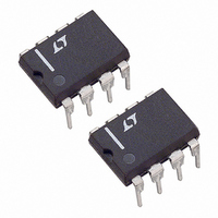
LTC660CN8 Linear Technology, LTC660CN8 Datasheet

LTC660CN8
Specifications of LTC660CN8
Available stocks
Related parts for LTC660CN8
LTC660CN8 Summary of contents
Page 1
... The oscillator runs at a 10kHz frequency when unloaded. A higher frequency outside the audio band can also be obtained if the BOOST pin is tied + The LTC660 contains an internal oscillator, divide-by-two, voltage level shifter and four power MOSFETs. , LTC and LT are registered trademarks of Linear Technology Corporation INPUT –5V OUTPUT ...
Page 2
... OUT to V for temperatures above 85 C, OUT must not be shorted to GND or V even instantaneously, or device damage may result INFORMATION ORDER PART TOP VIEW NUMBER + OSC LTC660CN8 LV 6 LTC660CS8 5 V OUT N8 PACKAGE S8 PART MARKING S8 PACKAGE 660 = 100 C/W ( 150 C/W (S) JA ...
Page 3
W U TYPICAL PERFORMANCE CHARACTERISTICS Supply Current vs Supply Voltage 300 250 200 150 + BOOST = V 100 BOOST = OPEN 50 0 1.5 2 2.5 3 3.5 4 4.5 5 5.5 SUPPLY VOLTAGE ...
Page 4
LTC660 W U TYPICAL PERFORMANCE CHARACTERISTICS Output Voltage Drop vs Load Current 1 0.9 BOOST = V 0.8 0 2.5V 0.6 0 1.5V 0 3.5V ...
Page 5
PIN FUNCTIONS PIN NAME INVERTER 1 BOOST Internal Oscillator Frequency Control Pin. BOOST = Open, f OSC + BOOST = OSC externally BOOST has no effect CAP Positive Terminal for Charge Pump ...
Page 6
LTC660 U U APPLICATIONS INFORMATION Theory of Operation To understand the theory of operation for the LTC660, a review of a basic switched-capacitor building block is helpful. In Figure 2, when the switch is in the left position, capacitor C1 ...
Page 7
U U APPLICATIONS INFORMATION + V 7.0I I BOOST (1) 7. (6) Figure 5. Oscillator By connecting the BOOST pin (Pin discharge current is increased and, hence, the frequency is increased by approximately four and ...
Page 8
LTC660 U TYPICAL APPLICATIONS Negative Voltage Converter Figure 7 shows a typical connection which will provide a negative supply from an available positive supply. This circuit operates over full temperature and power supply ranges without the need of any external ...
Page 9
U TYPICAL APPLICATIONS (9V LTC660 150 11V B Figure 10. Battery Splitter LTC660 3 C1 150 LTC660 + ...
Page 10
LTC660 PACKAGE DESCRIPTION 0.300 – 0.325 (7.620 – 8.255) 0.009 – 0.015 (0.229 – 0.381) +0.035 0.325 –0.015 +0.889 8.255 –0.381 *THESE DIMENSIONS DO NOT INCLUDE MOLD FLASH OR PROTRUSIONS. MOLD FLASH OR PROTRUSIONS SHALL NOT EXCEED 0.010 INCH (0.254mm) ...
Page 11
... FLASH SHALL NOT EXCEED 0.010" (0.254mm) PER SIDE Information furnished by Linear Technology Corporation is believed to be accurate and reliable. However, no responsibility is assumed for its use. Linear Technology Corporation makes no represen- tation that the interconnection of its circuits as described herein will not infringe on existing patent rights. ...
Page 12
... Lowest Cost 13V 20V Highest Voltage 16V Adjustable Output 6V 12V Fixed Output 9V – 4V, – 4.5V and Adjustable Outputs V IN 1. –V OUT IN LTC660 • F07 OUT IN C2 150 F LTC660 • F08 LT/GP 0598 2K REV A • PRINTED IN USA LINEAR TECHNOLOGY CORPORATION 1995 ...


