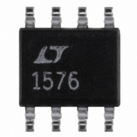
LT1576CS8-5SYNC#TRPBF Linear Technology, LT1576CS8-5SYNC#TRPBF Datasheet - Page 7

LT1576CS8-5SYNC#TRPBF
Manufacturer Part Number
LT1576CS8-5SYNC#TRPBF
Description
IC REG SW 5V 1.5A STEPDOWN 8SOIC
Manufacturer
Linear Technology
Type
Step-Down (Buck)r
Datasheet
1.LT1576CS8PBF.pdf
(28 pages)
Specifications of LT1576CS8-5SYNC#TRPBF
Internal Switch(s)
Yes
Synchronous Rectifier
No
Number Of Outputs
1
Voltage - Output
5V
Current - Output
1.5A
Frequency - Switching
200kHz
Voltage - Input
5 ~ 25 V
Operating Temperature
0°C ~ 125°C
Mounting Type
Surface Mount
Package / Case
8-SOIC (3.9mm Width)
Lead Free Status / RoHS Status
Lead free / RoHS Compliant
Power - Output
-
Available stocks
Company
Part Number
Manufacturer
Quantity
Price
Part Number:
LT1576CS8-5SYNC#TRPBFLT1576CS8-5SYNC#PBF
Manufacturer:
LINEAR/凌特
Quantity:
20 000
BLOCK
PIN
This pin sits at about 1V for very light loads and 2V at
maximum load. It can be driven to ground to shut off the
regulator, but if driven high, current must be limited to
4mA.
FB/SENSE (Pin 7): The feedback pin is the input to the
error amplifier which is referenced to an internal 1.21V
source. An external resistive divider is used to set the
output voltage. Three additional functions are performed
by the FB pin. The fixed voltage (-5) parts have the divider
resistors included on-chip and the FB pin is used as a
SENSE pin, connected directly to the 5V output. When the
pin voltage drops below 0.7V, the switch current limit and
the switching frequency are reduced and the external sync
function is disabled. See Feedback Pin Function section in
Applications Information for details.
The LT1576 is a constant frequency, current mode buck
converter. This means that there is an internal clock and
two feedback loops that control the duty cycle of the power
switch. In addition to the normal error amplifier, there is a
current sense amplifier that monitors switch current on a
cycle-by-cycle basis. A switch cycle starts with an oscilla-
tor pulse which sets the R
When switch current reaches a level set by the inverting
input of the comparator, the flip-flop is reset and the
switch turns off. Output voltage control is obtained by
using the output of the error amplifier to set the switch
current trip point. This technique means that the error
amplifier commands current to be delivered to the output
rather than voltage. A voltage fed system will have low
phase shift up to the resonant frequency of the inductor
and output capacitor, then an abrupt 180 shift will occur.
The current fed system will have 90 phase shift at a much
lower frequency, but will not have the additional 90 shift
until well beyond the LC resonant frequency. This makes
U
FUNCTIONS
U
DIAGRAM
U
S
W
flip-flop to turn the switch on.
SYNC (Pin 8): The SYNC pin is used to synchronize the
internal oscillator to an external signal. It is directly logic
compatible and can be driven with any signal between
10% and 90% duty cycle. The synchronizing range is
equal to initial operating frequency, up to 400kHz. This pin
replaces SHDN on -SYNC option parts. See Synchronizing
section in Applications Information for details.
SHDN (Pin 8): The shutdown pin is used to turn off the
regulator and to reduce input drain current to a few
microamperes. Actually, this pin has two separate thresh-
olds, one at 2.42V to disable switching, and a second at
0.37V to force complete micropower shutdown. The 2.42V
threshold functions as an accurate undervoltage lockout
(UVLO). This can be used to prevent the regulator from
operating until the input voltage has reached a predeter-
mined level.
it much easier to frequency compensate the feedback loop
and also gives much quicker transient response.
Most of the circuitry of the LT1576 operates from an
internal 2.9V bias line. The bias regulator normally draws
power from the regulator input pin, but if the BIAS pin is
connected to an external voltage higher than 3V, bias
power will be drawn from the external source (typically the
regulated output voltage). This will improve efficiency if
the BIAS pin voltage is lower than regulator input voltage.
High switch efficiency is attained by using the BOOST pin
to provide a voltage to the switch driver which is higher
than the input voltage, allowing the switch to saturate. This
boosted voltage is generated with an external capacitor
and diode. Two comparators are connected to the shut-
down pin. One has a 2.44V threshold for undervoltage
lockout and the second has a 0.4V threshold for complete
shutdown.
LT1576/LT1576-5
7


