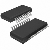
LTC1434CGN Linear Technology, LTC1434CGN Datasheet - Page 10

LTC1434CGN
Manufacturer Part Number
LTC1434CGN
Description
IC DC/DC CONV STEP-DOWN 20-SSOP
Manufacturer
Linear Technology
Type
Step-Down (Buck)r
Datasheet
1.LTC1433CGN.pdf
(20 pages)
Specifications of LTC1434CGN
Internal Switch(s)
Yes
Synchronous Rectifier
No
Number Of Outputs
1
Voltage - Output
3.3V, 5V, Adj
Current - Output
450mA
Frequency - Switching
125kHz ~ 240kHz
Voltage - Input
3 ~ 13.5 V
Operating Temperature
0°C ~ 70°C
Mounting Type
Surface Mount
Package / Case
20-SSOP
Lead Free Status / RoHS Status
Contains lead / RoHS non-compliant
Power - Output
-
APPLICATIONS
LTC1433/LTC1434
Efficiency Considerations
Since there are two separate pins for the drain of the small
and large P-channel switch, we could utilize two induc-
tors to further enhance the efficiency of the regulator over
the low load current range. Figure 4 shows the circuit
connection.(Also refer to the Typical Applications sec-
tion.)
To reduce core losses, the user can use a higher value
inductor on the small P-channel switch. Since this switch
only carries a small part of the overall current, the user can
still use a small physical size inductor without sacrificing
on copper losses. The Schottky diode can also be chosen
with a lower current rating. For the graph in Figure 5, a
Coilcraft DT1608C series inductor is used along with a
MBRS0520LT3 Schottky diode on the SSW pin. As can be
seen from Figure 5, the average efficiency gain over the
region where the small P-channel is on is about 3%.
10
Figure 4. Using Two Inductors for Higher Low Current Efficiency
Figure 5. Efficiency Comparison Between Single Inductor
and Dual Inductor
100
90
80
70
60
50
40
0.001
V
C
OUT
OSC
= 3.3V
= 47pF
LTC1433/
U
LTC1434
0.01
LOAD CURRENT (A)
INFORMATION
BSW
SSW
U
ONE 22 H INDUCTOR
ON SSW AND BSW
100 H ON SSW
22 H ON BSW
V
V
IN
IN
= 5V
= 9V
0.1
D1
D2
W
L1
L2
1433/34 • F05
1433/34 F04
1
U
Hence, the dual inductor configuration is good for the user
who requires as high an efficiency as possible at low load
while retaining constant frequency operation.
Output Voltage Programming
The LTC1433/LTC1434 family all have pin selectable out-
put voltage programming. The output voltage is selected
by the V
The LTC1433/LTC1434 family also has remote output
voltage sense capability. The top of the internal resistive
divider is internally connected to V
voltage applications, the V
output voltage as shown in Figure 6. When using an
external resistive divider, the V
the V
shown in Figure 7. To prevent stray pickup, a 100pF
capacitor is suggested across R1 located close to the
LTC1433/LTC1434.
Figure 6. LTC1433/LTC1434 Fixed Output Applications
OSENSE
Figure 7. LTC1433/LTC1434 Adjustable Applications
V
V
V
PROG
PROG =
PROG
PROG
V
= 0V
= Open (DC)
pin is connected to the feedback resistors as
LTC1433/
OUT
LTC1433/
LTC1434
LTC1434
V
pin as follows:
IN
= 1.19V 1 +
V
V
OSENSE
OSENSE
V
V
SGND
SGND
PROG
PROG
R2
R1
OSENSE
GND: V
V
OPEN (DC)
IN
: V
PROG
+
OUT
OUT
OSENSE
100pF
pin is connected to the
= 5V
C
= 3.3V
pin is left open DC and
OUT
V
V
V
OUT
OUT
OUT
= 3.3V
= 5V
= Adjustable
. For fixed output
1433/34 F06
R2
R1
V
OUT
1433/34 F07
V
OUT


