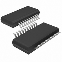
LTC1434CGN#PBF Linear Technology, LTC1434CGN#PBF Datasheet - Page 5

LTC1434CGN#PBF
Manufacturer Part Number
LTC1434CGN#PBF
Description
IC DC/DC CONV STEP-DOWN 20-SSOP
Manufacturer
Linear Technology
Type
Step-Down (Buck)r
Datasheet
1.LTC1433CGN.pdf
(20 pages)
Specifications of LTC1434CGN#PBF
Internal Switch(s)
Yes
Synchronous Rectifier
No
Number Of Outputs
1
Voltage - Output
3.3V, 5V, Adj
Current - Output
450mA
Frequency - Switching
125kHz ~ 240kHz
Voltage - Input
3 ~ 13.5 V
Operating Temperature
0°C ~ 70°C
Mounting Type
Surface Mount
Package / Case
20-SSOP
Lead Free Status / RoHS Status
Lead free / RoHS Compliant
Power - Output
-
PIN
SSW (Pin 1/Pin 2): Drain of the Small P-Channel MOSFET
Switch.
BSW (Pin 3/Pin 4): Drain of the Large P-Channel MOSFET
Switch.
SGND (Pin 5): Small-Signal Ground. Must be routed
separately from other grounds to the (–) terminal of C
RUN/SS (Pin 6/Pin 7): Combination of Soft Start and Run
Control Inputs. A capacitor to ground at this pin sets the
ramp time to full current output. The time is approxi-
mately 0.5s/ F. Forcing this pin below 1.3V causes all
circuitry to be shut down except the low-battery com-
parator. For input voltages above 6V this pin is clamped by
a 6V Zener (see Functional Diagram). Applying voltages
greater than 6V to this pin will cause additional current to
flow into this pin.
LBO (Pin 7/Pin 9): Open-Drain Output of an N-Channel
Pull-Down. This pin will sink current when LBI goes below
1.19V.
LBI (Pin 8/Pin 10): The (+) Input of the Low-Battery
Voltage Comparator. The (–) input is connected to the
1.19V reference. When LBI is grounded along with RUN/
SS, this comparator will shut down along with the rest of
the control circuitry. LBO will go to high impedance.
V
output voltage. When V
output is set to 3.3V and 5V respectively, with V
connected to the output. Leaving V
the output voltage to be set by an external resistive divider.
V
resistive divider.
V
voltage either from the output or from an external resistive
divider across the output. The V
which point V
PROG
OSENSE
OSENSE
U
FUNCTIONS
(Pin 9/Pin 11): The voltage at this pin selects the
V
V
V
PROG
PROG =
PROG
(Pin 10/Pin 12): This pin receives the feedback
is then connected to the common node of the
U
= 0V
= Open (DC)
V
OSENSE
IN
U
must be connected.
PROG
(LTC1433/LTC1434)
= 0V or V
PROG
PROG
V
V
V
OUT
OUT
OUT
pin determines at
open (DC) allows
= 3.3V
= 5V
= Adjustable
PROG
= V
OSENSE
IN
, the
OUT
.
I
The current comparator threshold increases with this
control voltage. Nominal voltage range for this pin is 0V
to 2.4V.
POR (Pin 12/Pin 14): Open-Drain Output of an N-Chan-
nel Pull-Down. This pin sinks current when the output
voltage is 7.5% out of regulation. When the output rises
to – 5% of its regulated value, the pin goes into high
impedance after 2
output is asserted when the device is in shutdown,
independent of V
C
tween this pin and ground to set the operating frequency.
PLL LPF (Pin 16 LTC1434): Output of the Phase Detector
and Control Input of the Oscillator. Normally a series RC
lowpass network is connected from this pin to ground. Tie
this pin to SGND in applications which do not use the
phase-locked loop. Can be driven by a 0V to 2.4V logic
signal for a frequency shifting option.
PLLIN (Pin 17 LTC1434): External Synchronizing Input to
the Phase Detector. This pin is internally terminated to
SGND with 50k . Tie this pin to SGND in applications
which do not use the phase-locked loop.
SV
Circuitry.
PGND (Pin 15/Pin 19): Switch Driver Ground. Connects to
the (–) terminal of C
be connected close to this pin.
PWRV
MOSFETs and Switch Drivers. Must decouple this pin
properly to ground.
NC (Pins 2, 4,/Pins 1, 3, 6, 8): No Connection.
TH
OSC
IN
(Pin 11/Pin 13): Error Amplifier Compensation Point.
(Pin 14/Pin 18): Main Supply for All the Control
(Pin 13/Pin 15): External capacitor connects be-
IN
(Pin 16/Pin 20): Supply for the Internal Power
OUT
16
IN
(65536) oscillator cycles. The POR
.
. Anode of the Schottky diode must
LTC1433/LTC1434
5


