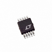
LT3757EMSE#PBF Linear Technology, LT3757EMSE#PBF Datasheet - Page 7

LT3757EMSE#PBF
Manufacturer Part Number
LT3757EMSE#PBF
Description
IC CTRLR DC/DC ADJ 10-MSOP
Manufacturer
Linear Technology
Type
Step-Up (Boost), Inverting, Flyback, Sepicr
Datasheet
1.LT3757EDDPBF.pdf
(36 pages)
Specifications of LT3757EMSE#PBF
Internal Switch(s)
No
Synchronous Rectifier
No
Number Of Outputs
1
Frequency - Switching
100kHz ~ 1MHz
Voltage - Input
2.9 ~ 40 V
Operating Temperature
-40°C ~ 125°C
Mounting Type
Surface Mount
Package / Case
10-MSOP Exposed Pad, 10-HMSOP, 10-eMSOP
Lead Free Status / RoHS Status
Lead free / RoHS Compliant
Current - Output
-
Voltage - Output
-
Power - Output
-
Available stocks
Company
Part Number
Manufacturer
Quantity
Price
pin FuncTions
VC (Pin 1): Error Amplifier Compensation Pin. Used to
stabilize the voltage loop with an external RC network.
FBX (Pin 2): Positive and Negative Feedback Pin. Receives
the feedback voltage from the external resistor divider
across the output. Also modulates the frequency during
start-up and fault conditions when FBX is close to GND.
SS (Pin 3): Soft-Start Pin. This pin modulates compensa-
tion pin voltage (VC) clamp. The soft-start interval is set
with an external capacitor. The pin has a 10µA (typical)
pull-up current source to an internal 2.5V rail. The soft-
start pin is reset to GND by an undervoltage condition
at SHDN/UVLO, an INTV
condition or an internal thermal lockout.
RT (Pin 4): Switching Frequency Adjustment Pin. Set the
frequency using a resistor to GND. Do not leave this pin
open.
SYNC (Pin 5): Frequency Synchronization Pin. Used to
synchronize the switching frequency to an outside clock.
If this feature is used, an R
program a switching frequency 20% slower than the SYNC
pulse frequency. Tie the SYNC pin to GND if this feature is
not used. SYNC is ignored when FBX is close to GND.
SENSE (Pin 6): The Current Sense Input for the Control
Loop. Kelvin connect this pin to the positive terminal of
the switch current sense resistor in the source of the
N-channel MOSFET. The negative terminal of the current
sense resistor should be connected to GND plane close
to the IC.
CC
T
undervoltage or overvoltage
resistor should be chosen to
GATE (Pin 7): N-Channel MOSFET Gate Driver Output.
Switches between INTV
IC is shut down, during thermal lockout or when INTV
above or below the OV or UV thresholds, respectively.
INTV
Gate Driver. Supplied from V
cal). INTV
capacitor placed close to pin. INTV
directly to V
be connected to a power supply whose voltage is higher
than 7.5V, and lower than V
not exceed 17.5V.
SHDN/UVLO (Pin 9): Shutdown and Undervoltage Detect
Pin. An accurate 1.22V (nominal) falling threshold with
externally programmable hysteresis detects when power
is okay to enable switching. Rising hysteresis is generated
by the external resistor divider and an accurate internal
2µA pull-down current. An undervoltage condition resets
sort-start. Tie to 0.4V, or less, to disable the device and
reduce V
V
with a 0.22µF , or larger, capacitor placed close to the
pin.
Exposed Pad (Pin 11): Ground. This pin also serves as the
negative terminal of the current sense resistor. The Exposed
Pad must be soldered directly to the local ground plane.
IN
(Pin 10): Input Supply Pin. Must be locally bypassed
CC
(Pin 8): Regulated Supply for Internal Loads and
IN
CC
quiescent current below 1µA.
must be bypassed with a minimum of 4.7µF
IN
, if V
IN
is less than 17.5V. INTV
CC
and GND. Driven to GND when
IN
IN
, provided that supply does
and regulated to 7.2V (typi-
CC
can be connected
LT3757
CC
can also
CC
3757fb
is


