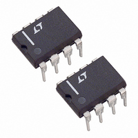
LT1376IN8-5 Linear Technology, LT1376IN8-5 Datasheet - Page 19

LT1376IN8-5
Manufacturer Part Number
LT1376IN8-5
Description
IC SW REG 1.5A 5V STEP-DWN 8-DIP
Manufacturer
Linear Technology
Type
Step-Down (Buck)r
Datasheet
1.LT1376CS8PBF.pdf
(28 pages)
Specifications of LT1376IN8-5
Internal Switch(s)
Yes
Synchronous Rectifier
No
Number Of Outputs
1
Voltage - Output
5V
Current - Output
1.5A
Frequency - Switching
500kHz
Voltage - Input
5 ~ 25 V
Operating Temperature
-40°C ~ 125°C
Mounting Type
Through Hole
Package / Case
8-DIP (0.300", 7.62mm)
Lead Free Status / RoHS Status
Contains lead / RoHS non-compliant
Power - Output
-
APPLICATIONS
SYNCHRONIZING (Available on LT1375 Only)
The LT1375 has the BIAS pin replaced with a SYNC pin,
which is used to synchronize the internal oscillator to an
external signal. It is directly logic compatible and can be
driven with any signal between 10% and 90% duty cycle.
The synchronizing range is equal to initial operating fre-
quency up to 900kHz. This means that minimum practical
sync frequency is equal to the worst-case high self-
oscillating frequency (560kHz), not the typical operating
frequency of 500kHz. Caution should be used when syn-
chronizing above 700kHz because at higher sync frequen-
cies the amplitude of the internal slope compensation
used to prevent subharmonic switching is reduced. This
type of subharmonic switching only occurs at input volt-
ages less than twice output voltage. Higher inductor
values will tend to eliminate problems. See Frequency
INPUT
8.0
7.5
7.0
6.5
6.0
5.5
5.0
+
0.001
Figure 10. Reducing Minimum Input Voltage
V
IN
Figure 9. Minimum Input Voltage
GND
LT1376-5
0.01
BOOST
LOAD CURRENT (A)
(D)
(C)
U
V
C
SENSE
(B)
V
C
0.1µF
INFORMATION
SW
C
U
C2
0.1
(A)
Q1
2N3905
W
D3
1N914
1N914
1
D1
(A) MINIMUM VOLTAGE
(B) MINIMUM VOLTAGE
(C) MINIMUM VOLTAGE
(D) MINIMUM VOLTAGE
L1
TO START WITH
STANDARD CIRCUIT
TO RUN WITH
STANDARD CIRCUIT
TO START WITH
PNP
TO RUN WITH
PNP
+
U
C1
1375/76 F09
OUTPUT
1375/76 F10
Compensation section for a discussion of an entirely
different cause of subharmonic switching before assum-
ing that the cause is insufficient slope compensation.
Application Note 19 has more details on the theory of slope
compensation.
There is a sync-supply sequence issue with the LT1375. If
power is supplied to the regulator after the external sync
signal is supplied, the regulator may not start. This is
caused by the internal frequency foldback condition that
occurs when the FB pin is below 1V (see block diagram
description in the data sheet). The oscillator tries to run at
100kHz when the FB pin is below 1V, and a high frequency
sync signal will then create an extremely low amplitude
oscillator waveform. This amplitude may be so low that the
switch logic is not triggered to create switching. Under the
normal regulated condition, the oscillator runs at much
higher amplitude with plenty of drive for the switch logic.
Note that for fixed voltage parts, the FB pin is replaced with
a SENSE pin, and the voltage divider resistors are internal.
In that case, the FB pin drops below 1V when the output
voltage is less than 40% of its regulated value.
There are no sequence problems if the power supply for
the sync signal comes from the output of the LT1375. If
this is not the case, and the sync signal could be present
when power is applied to the regulator, a gate should be
used to block sync signals as shown in Figure 11. Any
other technique which prevents sync signals when the
regulator output is low will work just as well. It does not
matter whether the sync signal is forced high or low; the
internal circuitry is edge triggered.
FREQUENCY COMPENSATION
Loop frequency compensation of switching regulators
can be a rather complicated problem because the reactive
components used to achieve high efficiency also
Figure 11. Gating the Sync Signal
V
IN
SYNC
LT1375
LT1375/LT1376
1375/76 F11
V
19
OUT
13756fd


