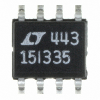
LTC1515IS8-3.3/5#TRPBF Linear Technology, LTC1515IS8-3.3/5#TRPBF Datasheet - Page 4

LTC1515IS8-3.3/5#TRPBF
Manufacturer Part Number
LTC1515IS8-3.3/5#TRPBF
Description
IC MULTI CONFIG 3.3V/5V 8SOIC
Manufacturer
Linear Technology
Type
Step-Down (Buck), Step-Up (Boost), Switched Capacitor (Charge Pump)r
Datasheet
1.LTC1515IS8PBF.pdf
(8 pages)
Specifications of LTC1515IS8-3.3/5#TRPBF
Internal Switch(s)
Yes
Synchronous Rectifier
No
Number Of Outputs
1
Voltage - Output
3.3V, 5V
Current - Output
50mA
Frequency - Switching
650kHz
Voltage - Input
2 ~ 10 V
Operating Temperature
-40°C ~ 85°C
Mounting Type
Surface Mount
Package / Case
8-SOIC (3.9mm Width)
Lead Free Status / RoHS Status
Lead free / RoHS Compliant
Power - Output
-
Available stocks
Company
Part Number
Manufacturer
Quantity
Price
pin may still be controlled with 3V logic without causing a
large rise in V
float; connect to V
POR (Pin 2): Open-Drain Power-On Reset Output. This pin
will pull low upon initial power-up, during shutdown or
until V
more than 200ms typ.
5/3 (LTC1515-X) (Pin 3): Output Voltage Select. A logic
high on the 5/3 pin will force V
LTC1515 Series
TYPICAL PERFORMANCE CHARACTERISTICS
PIN
SHDN (Pin 1): Shutdown Input. A logic low on the SHDN
pin puts the part into shutdown mode. A logic high (V
4
1.6V) enables the part. At high V
100
25
20
15
10
80
60
40
20
U
5
0
0
0
LTC1515-X
3V Efficiency vs Input Voltage
LTC1515-X Shutdown Supply
Current vs Input Voltage
OUT
SHDN = 0V
FUNCTIONS
has been within 6.5% of its regulated value for
U
2
2
IN
INPUT VOLTAGE (V)
INPUT VOLTAGE (V)
quiescent current. The SHDN pin may not
4
4
IN
if unused.
U
6
6
–40 C
V
I
T
OUT
A
OUT
25 C
= 25 C
W
= 10mA
8
8
OUT
= 3V
85 C
1515 G12
1515 G09
to regulate to 5V. A logic
U
10
10
IN
voltages, the SHDN
AC COUPLED
100mV/DIV
50mA/DIV
V
I
100
OUT
OUT
80
60
40
20
0
LTC1515-X Step-Down Mode
5V Load Transient Response
LTC1515-X
3.3V Efficiency vs Input Voltage
V
IN
= 8V, V
2
SHDN
OUT
INPUT VOLTAGE (V)
= 5V, C
4
OUT
low will force V
3.3/5). As with the SHDN pin, the 5/3 pin may be driven with
3V logic over the entire V
FB (LTC1515) (Pin 3): Feedback Input. The voltage on this
pin is compared to the internal reference voltage (1.232V)
to keep the output in regulation. An external resistor divider
is required between V
voltage. Total divider resistance should not exceed 2M.
GND (Pin 4): Ground. Should be tied to a ground plane for
best performance.
C1
Terminal.
= 10 F, T
–
6
(Pin 5): Charge Pump Flying Capacitor, Negative
V
I
TA = 25 C
OUT
OUT
A
= 25 C
= 10mA
8
= 3.3V
1515 G10
1515 G07
10
OUT
50mA
0mA
AC COUPLED
to 3V (LTC1515-3/5) or 3.3V (LTC1515-
100mV/DIV
50mA/DIV
OUT
V
I
100
IN
OUT
OUT
80
60
40
20
range. The 5/3 pin may not float.
2
LTC1515-X
5V Efficiency vs Input Voltage
LTC1515-X Step-Up Mode
5V Load Transient Response
V
and FB to adjust the output
IN
= 3.3V, V
4
OUT
INPUT VOLTAGE (V)
= 5V, C
6
OUT
= 10 F, T
8
V
I
TA = 25 C
OUT
OUT
A
10
= 10mA
= 25 C
= 5V
1515 G11
1515 G08
12


