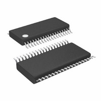
LTC3855IFE#PBF Linear Technology, LTC3855IFE#PBF Datasheet - Page 30

LTC3855IFE#PBF
Manufacturer Part Number
LTC3855IFE#PBF
Description
IC CTLR DC/DC MULTIPHASE 38SSOP
Manufacturer
Linear Technology
Series
PolyPhase®r
Type
Step-Down (Buck)r
Datasheet
1.LTC3855EUJPBF.pdf
(44 pages)
Specifications of LTC3855IFE#PBF
Internal Switch(s)
No
Synchronous Rectifier
Yes
Number Of Outputs
2
Voltage - Output
0.6 ~ 3.3 V, 0.6 ~ 12.5 V
Current - Output
25A
Frequency - Switching
250kHz ~ 770kHz
Voltage - Input
4.5 ~ 38 V
Operating Temperature
-40°C ~ 125°C
Mounting Type
Surface Mount
Package / Case
38-TSSOP Exposed Pad, 38-eTSSOP, 38-HTSSOP
Lead Free Status / RoHS Status
Lead free / RoHS Compliant
Power - Output
-
Available stocks
Company
Part Number
Manufacturer
Quantity
Price
LTC3855
applicaTions inForMaTion
PC Board Layout Checklist
When laying out the printed circuit board, the following
checklist should be used to ensure proper operation of
the IC. These items are also illustrated graphically in the
layout diagram of Figure 14. Figure 15 illustrates the
current waveforms present in the various branches of
the 2-phase synchronous regulators operating in the
continuous mode. Check the following in your layout:
1. Are the top N-channel MOSFETs M1 and M3 located
2. Are the signal and power grounds kept separate? The
3. Do the LTC3855 V
4. Are the SENSE
5. Is the INTV
0
within 1 cm of each other with a common drain con-
nection at C
coupling for the two channels as it can cause a large
resonant loop.
combined IC signal ground pin and the ground return
of C
minals. The V
possible. The path formed by the top N-channel MOSFET,
Schottky diode and the C
leads and PC trace lengths. The output capacitor (–)
terminals should be connected as close as possible
to the (–) terminals of the input capacitor by placing
the capacitors next to each other and away from the
Schottky loop described above.
the (+) terminals of C
connected between the (+) terminal of C
ground. The feedback resistor connections should not
be along the high current input feeds from the input
capacitor(s).
minimum PC trace spacing? The filter capacitor between
SENSE
to the IC. Ensure accurate current sensing with Kelvin
connections at the sense resistor or inductor, whichever
is used for current sensing.
the IC, between the INTV
This capacitor carries the MOSFET drivers current peaks.
An additional 1µF ceramic capacitor placed immediately
next to the INTV
noise performance substantially.
INTVCC
+
and SENSE
CC
must return to the combined C
IN
decoupling capacitor connected close to
FB
? Do not attempt to split the input de-
+
and SENSE
and I
CC
FB
and PGND pins can help improve
–
pins’ resistive dividers connect to
OUT
TH
should be as close as possible
CC
? The resistive divider must be
IN
traces should be as short as
and the power ground pins?
capacitor should have short
–
leads routed together with
OUT
OUT
and signal
(–) ter-
6. Keep the switching nodes (SW1, SW2), top gate nodes
7. Are DIFFP and DIFFN leads routed together and correctly
8. Use a modified “star ground” technique: a low imped-
PC Board Layout Debugging
Start with one controller at a time. It is helpful to use a
DC-50MHz current probe to monitor the current in the
inductor while testing the circuit. Monitor the output
switching node (SW pin) to synchronize the oscilloscope
to the internal oscillator and probe the actual output voltage
as well. Check for proper performance over the operating
voltage and current range expected in the application.
The frequency of operation should be maintained over
the input voltage range down to dropout and until the
output load drops below the low current operation
threshold—typically 10% of the maximum designed cur-
rent level in Burst Mode operation.
The duty cycle percentage should be maintained from
cycle to cycle in a well-designed, low noise PCB implemen-
tation. Variation in the duty cycle at a subharmonic rate
can suggest noise pickup at the current or voltage sensing
inputs or inadequate loop compensation. Overcompensa-
tion of the loop can be used to tame a poor PC layout if
regulator bandwidth optimization is not required. Only after
each controller is checked for its individual performance
should both controllers be turned on at the same time.
A particularly difficult region of operation is when one
controller channel is nearing its current comparator trip
point when the other channel is turning on its top MOSFET.
(TG1, TG2), and boost nodes (BOOST1, BOOST2) away
from sensitive small-signal nodes, especially from the
opposite channel’s voltage and current sensing feed-
back pins. All of these nodes have very large and fast
moving signals and therefore should be kept on the
“output side” of the LTC3855 and occupy minimum
PC trace area. If DCR sensing is used, place the top
resistor (Figure 2b, R1) close to the switching node.
Kelvin sensing the output voltage?
ance, large copper area central grounding point on
the same side of the PC board as the input and output
capacitors with tie-ins for the bottom of the INTV
decoupling capacitor, the bottom of the voltage feedback
resistive divider and the SGND pin of the IC.
3855f
CC


