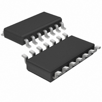
LTC1148HVCS-5#PBF Linear Technology, LTC1148HVCS-5#PBF Datasheet - Page 14

LTC1148HVCS-5#PBF
Manufacturer Part Number
LTC1148HVCS-5#PBF
Description
IC SW REG STEP-DOWN 5V 14-SOIC
Manufacturer
Linear Technology
Type
Step-Down (Buck)r
Datasheet
1.LTC1148CSPBF.pdf
(20 pages)
Specifications of LTC1148HVCS-5#PBF
Internal Switch(s)
No
Synchronous Rectifier
Yes
Number Of Outputs
1
Voltage - Output
5V
Current - Output
50mA
Frequency - Switching
250kHz
Voltage - Input
3.5 ~ 20 V
Operating Temperature
0°C ~ 70°C
Mounting Type
Surface Mount
Package / Case
14-SOIC (3.9mm Width), 14-SOL
Lead Free Status / RoHS Status
Lead free / RoHS Compliant
Power - Output
-
Available stocks
Company
Part Number
Manufacturer
Quantity
Price
APPLICATIO S I FOR ATIO
LTC1148
LTC1148-3.3/LTC1148-5
14
With the addition of R3, a current is generated through R1
causing an offset of:
If V
celled and Burst Mode operation is prevented from occur-
ring. Since V
is also decreased by the same offset. Thus, to get back to
the same I
lower:
To prevent noise spikes from erroneously tripping the
current comparator, a 1000pF capacitor is needed across
Pins 7 and 8.
Output Crowbar
An added feature to using an N-channel MOSFET as the
synchronous switch is the ability to crowbar the output
with the same MOSFET. Pulling the timing capacitor Pin
4 above 1.5V when the output voltage is greater than the
desired regulated value will turn “on” the N-channel
MOSFET.
A fault condition which causes the output voltage to go
above a maximum allowable value can be detected by
external circuitry. Turning on the N-channel MOSFET
when this fault is detected will cause large currents to flow
and blow the system fuse.
The N-channel MOSFET needs to be sized so it will safely
handle this overcurrent condition. The typical delay from
pulling the C
is 250ns. Note: Under shutdown conditions, the N-chan-
nel is held OFF and pulling the C
the N-channel MOSFET to crowbar the output.
A simple N-channel FET can be used as an interface
between the overvoltage detect circuitry and the LTC1148
as shown in Figure 7.
V
R
OFFSET
OFFSET
SENSE
> 25mV, the minimum threshold will be can-
MAX
≈ 75mV
= V
OFFSET
T
pin high and the N drive Pin 14 going high
I
, the value of the sense resistor must be
MAX
OUT
is constant, the maximum load current
)
U U
R1 + R3
R1
)
T
pin high will not cause
W
U
Troubleshooting Hints
Since efficiency is critical to LTC1148 series applications,
it is very important to verify that the circuit is functioning
correctly in both continuous and Burst Mode operation.
The waveform to monitor is the voltage on the timing
capacitor Pin 4.
In continuous mode (I
pin should be a sawtooth with a 0.9V
voltage should never dip below 2V as shown in Figure 8a.
When load currents are low (I
operation should occur with the C
cally falling to ground as shown in Figure 8b.
If Pin 4 is observed falling to ground at high output
currents, it indicates poor decoupling or improper ground-
ing. Refer to the Board Layout Checklist.
FROM CROWBAR DETECT CIRCUIT
OFF WHEN V
(ACTIVE WHEN V
Figure 7. Output Crowbar Interface
GATE
(a) CONTINUOUS MODE OPERATION
= GROUND)
Figure 8. C
GATE
(b) Burst Mode OPERATION
= V
LOAD
IN
> I
T
Waveforms
BURST
LOAD
T
VN2222LL
pin waveform periodi-
) the voltage on the C
< I
BURST
5
4
P-P
INTV
C
LTC1148
T
) Burst Mode
swing. This
LTC1148 • F07
CC
114835fd
LTC1148 • F08
3.3V
0V
3.3V
0V
T


