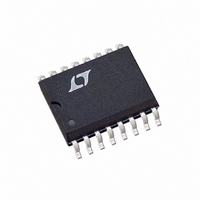
LTC1149CS-5 Linear Technology, LTC1149CS-5 Datasheet - Page 5

LTC1149CS-5
Manufacturer Part Number
LTC1149CS-5
Description
IC SW REG STEP-DOWN 5V 16-SOIC
Manufacturer
Linear Technology
Type
Step-Down (Buck)r
Datasheet
1.LTC1149CNPBF.pdf
(20 pages)
Specifications of LTC1149CS-5
Internal Switch(s)
No
Synchronous Rectifier
Yes
Number Of Outputs
1
Voltage - Output
5V
Current - Output
50mA
Frequency - Switching
250kHz
Voltage - Input
0 ~ 48 V
Operating Temperature
0°C ~ 70°C
Mounting Type
Surface Mount
Package / Case
16-SOIC (3.9mm Width)
Lead Free Status / RoHS Status
Contains lead / RoHS non-compliant
Power - Output
-
Available stocks
Company
Part Number
Manufacturer
Quantity
Price
Part Number:
LTC1149CS-5
Manufacturer:
LINEAR/凌特
Quantity:
20 000
Part Number:
LTC1149CS-5#TRPBF
Manufacturer:
LINEAR/凌特
Quantity:
20 000
OPERATIO
PI FU CTIO S
PGATE (Pin 1): Level-Shifted Gate Drive Signal for Top
P-Channel MOSFET. The voltage swing at Pin 1 is from V
to V
V
V
3 is not protected against DC short circuits.
PDRIVE (Pin 4): High Current Gate Drive for Top
P-Channel MOSFET. The voltage swing at Pin 4 is from V
to ground.
V
Supplies. Must be closely decoupled to power ground.
C
the operating frequency. (The frequency is also dependent
on the ratio V
I
comparator threshold increases with the Pin 7 voltage.
SENSE
which sets the output voltage in LTC1149-3.3 and
LTC1149-5 versions. Pin 8 is also the (–) input for the
current comparator.
SENSE
A built-in offset between Pins 8 and 9 in conjunction with
R
The LTC1149 series uses a current mode, constant off-
time architecture to synchronously switch an external pair
of complementary power MOSFETs. Operating frequency
is set by an external capacitor at the timing capacitor,
Pin 6.
The output voltage is sensed either by an internal voltage
divider connected to SENSE
LTC1149-5) or an external divider returned to V
(LTC1149). A voltage comparator V, and a gain block G,
compare the divided output voltage with a reference
voltage of 1.25V. To optimize efficiency, the LTC1149
series automatically switches between two modes of
operation, burst and continuous. The voltage comparator
is the primary control element for Burst Mode operation,
while the gain block controls the output voltage in continu-
ous mode.
TH
IN
CC
CC
T
SENSE
(Pin 6): External capacitor C
U
(Pin 7): Gain Amplifier Decoupling Point. The current
(Pin 2): Main Supply Input Pin.
IN
(Pin 3): Output Pin of Low Dropout 10V Regulator. Pin
(Pin 5): Regulated 10V Input for Driver and Control
– V
+
–
sets the current trip threshold.
(Pin 9): The (+) Input for the Current Comparator.
(Pin 8): Connects to internal resistive divider
CC
U
.
OUT
/V
U
IN
U
.)
(Refer to Functional Diagram)
–
, Pin 8 (LTC1149-3.3 and
T
from Pin 6 to ground sets
FB
Pin 10
CC
IN
SHDN1/V
10 serves as a shutdown pin for the control circuitry only
(V
LTC1149-5 high holds both MOSFETs off. Must be at
ground potential for normal operation.
For the LTC1149 adjustable version, Pin 10 serves as the
feedback pin from an external resistive divider used to set
the output voltage.
SGND (Pin 11): Small-Signal Ground. Must be routed
separately from other grounds to the (–) terminal of C
PGND (Pin 12): Driver Power Ground. Connects to source
of N-channel MOSFET and the (–) terminal of C
NGATE (Pin 13): High Current Drive for Bottom
N-channel MOSFET. The voltage swing at Pin 13 is from
ground to V
RGND (Pin 14): Low Dropout Regulator Ground. Con-
nects to power ground.
SHDN2 (Pin 15): Master Shutdown Pin. Taking Pin 15
high shuts down V
logic signal with t
CAP (Pin 16): Charge Compensation Pin. A capacitor from
Pin 16 to V
level-shift capacitor during supply transitions. The Pin 16
capacitor must be larger than the Pin 4 capacitor .
A low dropout 10V regulator provides the operating volt-
age V
driver outputs at Pins 4 and 13 are referenced to ground,
which fulfills the N-channel MOSFET gate drive require-
ment. The P-channel gate drive at Pin 1 must be refer-
enced to the main supply input V
by level-shifting the Pin 4 signal via an internal 500k
resistor and external capacitor.
During the switch “ON” cycle in continuous mode, current
comparator C monitors the voltage between Pins 8 and 9
connected across an external shunt in series with the
inductor. When the voltage across the shunt reaches its
threshold value, the PGATE output is switched to V
turning off the P-channel MOSFET. The timing capacitor
connected to Pin 6 is now allowed to discharge at a rate
determined by the off-time controller. The discharge
CC
is not affected). Taking Pin 10 of the LTC1149-3.3 or
CC
for the MOSFET drivers and control circuitry. The
FB
CC
(Pin 10): In fixed output voltage versions, Pin
CC
provides the charge required by the P-drive
.
LTC1149-3.3/LTC1149-5
r
, t
CC
f
< 1 s.
and all control circuitry; requires a
IN
, which is accomplished
LTC1149
IN
.
OUT
5
IN
.
,


