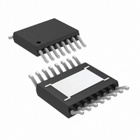
LT3500IMSE#TRPBF Linear Technology, LT3500IMSE#TRPBF Datasheet - Page 13

LT3500IMSE#TRPBF
Manufacturer Part Number
LT3500IMSE#TRPBF
Description
IC REG STEP-DOWN 2A 16-MSOP
Manufacturer
Linear Technology
Type
Step-Down (Buck)r
Datasheet
1.LT3500EDDPBF.pdf
(28 pages)
Specifications of LT3500IMSE#TRPBF
Topology
Step-Down (Buck) (1), Linear (LDO) (1)
Function
Any Function
Number Of Outputs
2
Frequency - Switching
500kHz ~ 2.4MHz
Voltage/current - Output 1
0.8 ~ 38.9 V, 2A
Voltage/current - Output 2
Adjustable, 13mA
W/led Driver
No
W/supervisor
No
W/sequencer
No
Voltage - Supply
3 V ~ 36 V
Operating Temperature
-40°C ~ 125°C
Mounting Type
Surface Mount
Package / Case
16-MSOP Exposed Pad
Current - Output
2A
Voltage - Output
0.8 ~ 38.9 V
Voltage - Input
3 ~ 36 V
Internal Switch(s)
Yes
Synchronous Rectifier
No
Lead Free Status / RoHS Status
Lead free / RoHS Compliant
Power - Output
-
Available stocks
Company
Part Number
Manufacturer
Quantity
Price
APPLICATIONS INFORMATION
Note that the LT3500 will regulate if the input voltage is
taken above the calculated maximum voltage as long as
maximum ratings of the V
However operation in this region of input voltage will exhibit
pulse skipping behavior.
Example:
Inductor Selection and Maximum Output Current
A good fi rst choice for the inductor value is:
where f is frequency in MHz and L is in μH.
With this value the maximum load current will be ~2A,
independent of input voltage. The inductor’s RMS current
rating must be greater than your maximum load current
and its saturation current should be about 30% higher. To
keep effi ciency high, the series resistance (DCR) should
be less than 0.05Ω.
V
Temperature = 25°C,
V
t
DC
DC
L =
V
V
OFF(MIN)
OUT1
SW
IN(MIN)
IN(MAX)
MAX
MIN
(V
= 0.3V, V
IN
= 3.3V, I
= t
= 1− (110ns)1MHz = 89%
=
− V
= 110ns
=
ON(MIN)
3.3 + 0.4
3.3 + 0.4
V
OUT1
0.89
IN
D
0.15
OUT1
• f
= 0.4V, t
) • V
• Frequency = 15%
= 1A, Frequency = 1MHz,
− 0.4 + 0.3 = 4.06V
OUT1
− 0.4 + 0.3 = 24.57V
IN
ON(MIN)
and BST pins are not violated.
= 150ns,
For applications with a duty cycle of about 50%, the induc-
tor value should be chosen to obtain an inductor ripple
current less than 40% of peak switch current.
Of course, such a simple design guide will not always result
in the optimum inductor for your application. A larger value
provides a slightly higher maximum load current, and will
reduce the output voltage ripple. If your load is lower than
1.5A, then you can decrease the value of the inductor and
operate with higher ripple current. This allows you to use
a physically smaller inductor, or one with a lower DCR
resulting in higher effi ciency.
The current in the inductor is a triangle wave with an
average value equal to the load current. The peak switch
current is equal to the output current plus half the peak-to
peak inductor ripple current. The LT3500 limits its switch
current in order to protect itself and the system from
overload faults. Therefore, the maximum output current
that the LT3500 will deliver depends on the current limit,
the inductor value, switch frequency, and the input and
output voltages. The inductor is chosen based on output
current requirements, output voltage ripple requirements,
size restrictions and effi ciency goals.
When the switch is off, the inductor sees the output volt-
age plus the catch diode drop. This gives the peak-to-peak
ripple current in the inductor:
where f is the switching frequency of the LT3500 and L
is the value of the inductor. The peak inductor and switch
current is:
I
ΔI
SW(PK)
L
=
(
1− DC
=I
LPK
)
(
=I
L • f
V
OUT1
OUT1
+ V
+
ΔI
D
2
)
L
LT3500
13
3500fc


