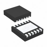
LT3500HDD#TRPBF Linear Technology, LT3500HDD#TRPBF Datasheet - Page 21

LT3500HDD#TRPBF
Manufacturer Part Number
LT3500HDD#TRPBF
Description
IC REG STP-DWN 2A 12-DFN
Manufacturer
Linear Technology
Type
Step-Down (Buck)r
Datasheet
1.LT3500EDDPBF.pdf
(28 pages)
Specifications of LT3500HDD#TRPBF
Topology
Step-Down (Buck) (1), Linear (LDO) (1)
Function
Any Function
Number Of Outputs
2
Frequency - Switching
500kHz ~ 2.4MHz
Voltage/current - Output 1
0.8 ~ 38.9 V, 2A
Voltage/current - Output 2
Adjustable, 13mA
W/led Driver
No
W/supervisor
No
W/sequencer
No
Voltage - Supply
3 V ~ 36 V
Operating Temperature
-40°C ~ 150°C
Mounting Type
Surface Mount
Package / Case
12-DFN
Current - Output
2A
Voltage - Output
0.8 ~ 38.9 V
Voltage - Input
3 ~ 36 V
Internal Switch(s)
Yes
Synchronous Rectifier
No
Lead Free Status / RoHS Status
Lead free / RoHS Compliant
Power - Output
-
Available stocks
Company
Part Number
Manufacturer
Quantity
Price
APPLICATIONS INFORMATION
At power-up, a reset signal sets the soft-start latch and
discharges the SS pin to approximately 0V to ensure
proper start-up. When the SS pin is fully discharged the
latch is reset and the internal 2.75μA current source starts
to charge the SS pin.
When the SS pin voltage is below 100mV, the V
pulled low which disables switching. As the SS pin voltage
rises above 100mV, the V
are regulated to the SS voltage. When the SS pin voltage
minus 100mV exceeds the internal 0.8V reference, the
outputs are regulated to the reference. The SS pin voltage
will continue to rise until it is clamped at 2V.
In the event of a V
driven below 0.8V, or the internal die temperature exceeding
its maximum rating during normal operation, the soft-start
latch is set, triggering a start-up sequence.
In addition, if the load exceeds the maximum output switch
current (switching regulator only), the output will start to
drop causing the V
the V
a result, the output will be regulated to the highest volt-
age that the maximum output current can support. For
example, if a 6V output is loaded by 1Ω the SS pin will
drop to 0.5V, regulating the output at 3V (typical current
limit time load, 3A • 1Ω). Once the overload condition is
removed, the output will soft-start from the temporary
voltage level to the normal regulation point.
Since the SS pin is clamped at 2V and has to discharge to
0.9V before taking control of regulation, momentary over-
load conditions will be tolerated without a soft-start recov-
ery. The typical time before the SS pin takes control is:
Power Good Indicators
The PG and PG pins are collector outputs of an internal
comparator. The comparator compares the voltages of
the FB and LFB pins to 90% of the reference voltage with
30mV of hysterisis.
t
SS(CONTROL)
C
pin is clamped, the SS pin will be discharged. As
=
IN
C
C
SS
pin clamp to be activated. As long as
600μA
undervoltage lockout, the SHDN pin
• 1.1V
C
pin is released and the outputs
C
pin is
The PG pin has a sink capability of 400μA when the FB and
LFB pins are below the threshold and can withstand 40V
when the outputs are in regulation. The PG pin is typically
connected to the output with a resistor and is used as an
error fl ag. The resistor value should be chosen to allow the
PG voltage to drop below 0.4V in an error condition.
Example:
The PG pin has a sink capability of 800μA when the FB
and LFB pins are above the threshold and can withstand
40V when the outputs are not in regulation. The PG pin is
typically used as a drive signal for an output disconnect
device. The PG pull-up resistor should be sized in the
same manner as the PG pull-up resistor.
Linear Regulator
The LT3500 contains an error amplifi er and a NPN output
device which can be confi gured as a linear regulator or as
a linear regulator controller.
With the LFB and LDRV pins confi gured as shown in
Figure 1, the LDRV pin outputs a regulated voltage with a
typical current limit of 13mA.
The LDRV voltage is programmed with a resistor divider
between the output and the LFB pin. Choose the 1% resis-
tors according to:
R4 should be 10.0k or less to avoid bias current errors.
Reference designators refer to the Block Diagram in
Figure 1.
The reference voltage for the linear regulator (LFB pin)
will track the SS pin in the same manner as the FB pin of
the switching regulator.
V
R
R3 = R4
OUT1
PG
= (5 – 0.4)/200μA = 23kΩ
= 5V, PGSINK
V
0.8V
LDRV
– 1
(MIN)
= 200μA
LT3500
21
3500fc


