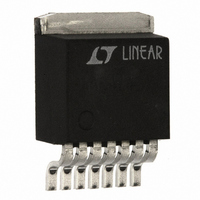
LT1506CR-3.3 Linear Technology, LT1506CR-3.3 Datasheet - Page 23

LT1506CR-3.3
Manufacturer Part Number
LT1506CR-3.3
Description
IC SW REG STEP-DOWN 500KHZ 7-DD
Manufacturer
Linear Technology
Type
Step-Down (Buck)r
Datasheet
1.LT1506CS8-3.3PBF.pdf
(24 pages)
Specifications of LT1506CR-3.3
Internal Switch(s)
Yes
Synchronous Rectifier
No
Number Of Outputs
1
Voltage - Output
3.3V
Current - Output
4.5A
Frequency - Switching
500kHz
Voltage - Input
4 ~ 15 V
Operating Temperature
0°C ~ 125°C
Mounting Type
Surface Mount
Package / Case
D²Pak, TO-263 (7 leads + tab)
Lead Free Status / RoHS Status
Contains lead / RoHS non-compliant
Power - Output
-
Available stocks
Company
Part Number
Manufacturer
Quantity
Price
Company:
Part Number:
LT1506CR-3.3
Manufacturer:
LT
Quantity:
5
Company:
Part Number:
LT1506CR-3.3
Manufacturer:
LT
Quantity:
5 510
Company:
Part Number:
LT1506CR-3.3
Manufacturer:
MOT
Quantity:
5 510
Part Number:
LT1506CR-3.3
Manufacturer:
LT/凌特
Quantity:
20 000
Company:
Part Number:
LT1506CR-3.3#TRPBF
Manufacturer:
TI
Quantity:
110
Part Number:
LT1506CR-3.3#TRPBF
Manufacturer:
LT/凌特
Quantity:
20 000
Company:
Part Number:
LT1506CR-3.3/IR
Manufacturer:
LT
Quantity:
500
APPLICATIONS
Redundant Operation
The circuit shown in Figure 15 is fault tolerant when
operating at less than 8A of output current. If one device
fails, the output will remain in regulation. The feedback
loop will compensate by raising the voltage on the V
increasing switch current of the two remaining devices.
BUCK CONVERTER WITH ADJUSTABLE SOFT START
Large capacitive loads can cause high input currents at
start-up. Figure 16 shows a circuit that limits the dv/dt of
the output at start-up, controlling the capacitor charge
rate. The buck converter is a typical configuration with the
addition of R3, R4, C
Q1 turns on, regulating switch current via the V
maintain a constant dv/dt at the output. Output rise time is
controlled by the current through C
Q1’s V
the circuit operates normally. R3 is transient protection for
the base of Q1.
Using the values shown in Figure 16,
The ramp is linear and rise times in the order of 100ms are
possible. Since the circuit is voltage controlled, the ramp
rate is unaffected by load characteristics and maximum
INPUT
12V
RiseTime
RiseTime
+
Figure 16. Buck Converter with Adjustable Soft Start
BE
. Once the output is in regulation, Q1 turns off and
C3
10 F
V
SHDN
IN
( )(
(
R
GND
47 10
LT1506
BOOST
4
U
•
SS
C
V
(
C
SS
V
and Q1. As the output starts to rise,
3
V
BE
C
1.5nF
SW
0.33 F
FB
INFORMATION
)(
)(
C
U
0 7
)
15 10
V
C2
.
D1
OUT
Q1
Information furnished by Linear Technology Corporation is believed to be accurate and reliable.
However, no responsibility is assumed for its use. Linear Technology Corporation makes no represen-
tation that the interconnection of its circuits as described herein will not infringe on existing patent rights.
•
)
1N914
100 F
–
5 H
D2
L1
9
R4
47k
W
SS
C1
)( )
R3
2k
5
defined by R4 and
15nF
C
SS
5
ms
R1
5.36k
R2
4.99k
1506 F16
U
C
pin to
C
OUTPUT
5V
4A
pin,
output current is unchanged. Variants of this circuit can be
used for sequencing multiple regulator outputs.
Dual Output SEPIC Converter
The circuit in Figure 17 generates both positive and
negative 5V outputs with a single piece of magnetics. The
two inductors shown are actually just two windings on a
standard B H Electronics inductor. The topology for the 5V
output is a standard buck converter. The – 5V topology
would be a simple flyback winding coupled to the buck
converter if C4 were not present. C4 creates a SEPIC
(Single-Ended Primary Inductance Converter) topology
whicn improves regulation and reduces ripple current in
L1. Without C4, the voltage swing on L1B compared to
L1A would vary due to relative loading and coupling
losses. C4 provides a low impedance path to maintain an
equal voltage swing in L1B, improving regulation. In a
flyback converter, during switch on time, all the converter’s
energy is stroed in L1A only, since no current flows in L1B.
At switch off, energy is transferred by magnetic coupling
into L1B, powering the – 5V rail. C4 pulls L1B positive
during switch on time, causing current to flow, and energy
to build in L1B and C4. At switch off, the energy stored in
both L1B and C4 supply the –5V rail. This reduces the
current in L1A and changes L1B current waveform from
square to triangular. For details on this circuit see Design
Note 100.
6V TO 15V
** TOKIN IE475ZY5U-C304
* L1 IS A SINGLE CORE WITH TWO WINDINGS
†
BH ELECTRONICS #501-0726
IF LOAD CAN GO TO ZERO, AN OPTIONAL
PRELOAD OF 1k TO 5k MAY BE USED TO
IMPROVE LOAD REGULATION
D1, D3: MBRD340
INPUT
GND
+
Figure 17. Dual Output SEPIC Converter
C3
10 F
25V
CERAMIC
V
SHDN
IN
GND
LT1506
BOOST
V
C
4.7 F
C4**
V
C
1.5nF
SW
FB
0.27 F
C
+
C2
L1*
D1
D3
1N914
6.8 H
10V TANT
L1*
D2
5.36k
4.99k
100 F
R1
R2
C5**
LT1506
+
+
C1**
100 F
10V TANT
23
OUTPUT
5V
OUTPUT
–5V
1506 F17
†


