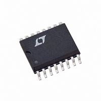
LTC1266ACS#TR Linear Technology, LTC1266ACS#TR Datasheet - Page 7

LTC1266ACS#TR
Manufacturer Part Number
LTC1266ACS#TR
Description
IC CTRLR SW REG SYNC ADJ 16SOIC
Manufacturer
Linear Technology
Type
Step-Down (Buck), Step-Up (Boost)r
Datasheet
1.LTC1266CSPBF.pdf
(20 pages)
Specifications of LTC1266ACS#TR
Internal Switch(s)
No
Synchronous Rectifier
Yes
Number Of Outputs
1
Voltage - Output
Adjustable
Current - Output
50mA
Frequency - Switching
400kHz
Voltage - Input
3.5 ~ 18 V
Operating Temperature
0°C ~ 70°C
Mounting Type
Surface Mount
Package / Case
16-SOIC (3.9mm Width)
Lead Free Status / RoHS Status
Contains lead / RoHS non-compliant
Power - Output
-
Available stocks
Company
Part Number
Manufacturer
Quantity
Price
FU CTIO AL DIAGRA
OPERATIO
The LTC1266 series uses a current mode, constant off-
time architecture to synchronously switch an external pair
of power MOSFETs. Operating frequency is set by an
external capacitor at the timing capacitor Pin 6.
The output voltage is sensed by an internal voltage divider
connected to SENSE
5) or external divider returned to V
A voltage comparator V, and a gain block G, compare the
divided output voltage with a reference voltage of 1.265V.
To optimize efficiency, the LTC1266 automatically switches
between two modes of operation, burst and continuous.
The voltage comparator is the primary control element
when the device is in Burst Mode operation, while the gain
block controls the output voltage in continuous mode.
U
SLEEP
GROUND
SIGNAL
S
12
+
–
U
V
U
TH2
–
C
6
, Pin 8, (LTC1266-3.3 and LTC1266-
T
V
TH1
–
+
V
IN
Q
CONTROL
T
OFF-TIME
FB
W
R
S
REFERENCE
PWR V
, Pin 10, (LTC1266).
LB
1.25V
IN
Pin 10 Connection Shown for LTC1266-3.3 and LTC1266-5; Changes Create LTC1266
IN
13
2
V
SENSE
V
IN
FB
–
+
–
LB
CONTROL
ON-TIME
ENABLE
MAX
16
15 PGND
BDRIVE
During the switch ON cycle in continuous mode, current
comparator C monitors the voltage between Pins 8 and 9
connected across an external shunt in series with the
inductor. When the voltage across the shunt reaches its
threshold value, the topside driver output is switched to
turn off the topside MOFSET (Power V
ground for N-channel). The timing capacitor connected to
Pin 6 is now allowed to discharge at a rate determined by
the off-time controller. The discharge current is made
proportional to the output voltage (measured by Pin 8) to
model the inductor current, which decays at a rate which
is also proportional to the output voltage. While the timing
capacitor is discharging, the bottom-side drive output is
switched to power V
N-channel MOSFET.
PINV
3
C
PINV
BINH
14
–
+
1
LB
I
TH
TDRIVE
OUT
4
7
–
LTC1266-3.3/LTC1266-5
+
13k
V
TRIP
SHDN
IN
11
V
to turn on the bottom-side
G
–
+
–
+
REFERENCE
SENSE
1.265V
9
V
OS
IN
+
ADJUSTABLE
VERSION
for P-channel or
5
V
10
LTC1266
FB
V
IN
SENSE
8
100k
–
7
1266 FD
5pF


