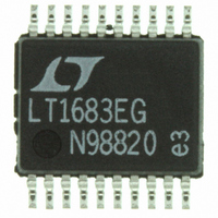
LTC1159CG#TR Linear Technology, LTC1159CG#TR Datasheet - Page 15

LTC1159CG#TR
Manufacturer Part Number
LTC1159CG#TR
Description
IC REG SW STPDWN SYNC ADJ 20SSOP
Manufacturer
Linear Technology
Type
Step-Down (Buck)r
Datasheet
1.LTC1159CSPBF.pdf
(20 pages)
Specifications of LTC1159CG#TR
Internal Switch(s)
No
Synchronous Rectifier
Yes
Number Of Outputs
1
Voltage - Output
Adjustable
Current - Output
50mA
Frequency - Switching
250kHz
Voltage - Input
4 ~ 40 V
Operating Temperature
0°C ~ 70°C
Mounting Type
Surface Mount
Package / Case
20-SSOP
Lead Free Status / RoHS Status
Contains lead / RoHS non-compliant
Power - Output
-
Available stocks
Company
Part Number
Manufacturer
Quantity
Price
APPLICATIO S I FOR ATIO
1) Are the signal and power grounds segregated? The
LTC1159 signal ground must connect separately to the
(–) plate of C
the source of the N-channel MOSFET, anode of the Schot-
tky diode and (–) plate of C
lead lengths as possible.
2) Does the LTC1159 SENSE
to R
tions, the resistive divider R1, R2 must be connected
between the (+) plate of C
3) Are the SENSE
with minimum PC trace spacing? The differential
decoupling capacitor between the two SENSE pins should
be as close as possible to the LTC1159. Up to 100 may
be placed in series with each sense lead to help decouple
the SENSE pins. However, when these resistors are used,
the capacitor should be no larger than 1000pF.
4) Does the (+) plate of C
P-channel MOSFET as closely as possible? An additional
0.1 F ceramic capacitor between V
may be required in some applications.
5) Is the V
tween the V
This capacitor carries the MOSFET driver peak currents.
6) In adjustable versions, the feedback pin is very sensitive
to pickup from the switch node. Care must be taken to
isolate V
tor switch signal.
SENSE
FB
and the (+) plate of C
CC
from possible capacitive coupling of the induc-
CC
OUT
decoupling capacitor connected closely be-
pins of the LTC1159 and power ground?
. The other ground pin(s) should return to
–
U
and SENSE
U
IN
OUT
IN
connect to the source of the
–
, which should have as short
pin connect to a point close
and signal ground.
OUT
+
? In adjustable applica-
leads routed together
W
IN
and power ground
U
7) Is the SHDN1 pin actively pulled to ground during
normal operation? SHDN1 is a high impedance pin and
must not be allowed to float.
Troubleshooting Hints
Since efficiency is critical to LTC1159 applications it is very
important to verify that the circuit is functioning correctly
in both continuous and Burst Mode operation. The wave-
form to monitor is the voltage on the C
In continuous mode (I
a sawtooth with a 0.9V
dip below 2V as shown in Figure 9a. When the load current
is low (I
with the C
shown in Figure 9b.
If the C
currents, it indicates poor decoupling or improper ground-
ing. Refer to the Board Layout Checklist.
T
LOAD
pin is observed falling to ground at high output
T
< I
waveform periodically falling to ground as
(a) CONTINUOUS MODE OPERATION
BURST
Figure 9. C
LTC1159-3.3/LTC1159-5
(b) Burst Mode OPERATION
), Burst Mode operation should occur
LOAD
P-P
swing. This voltage should never
T
Pin 6 Waveforms
> I
BURST
) the voltage should be
T
pin .
LTC1159
15
LTC1159 • F09
3.3V
0V
3.3V
0V


