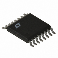
LT1765EFE Linear Technology, LT1765EFE Datasheet - Page 6

LT1765EFE
Manufacturer Part Number
LT1765EFE
Description
IC SW REG STEP-DOWN 3A 16-TSSOP
Manufacturer
Linear Technology
Type
Step-Down (Buck)r
Datasheet
1.LT1765ES8PBF.pdf
(20 pages)
Specifications of LT1765EFE
Internal Switch(s)
Yes
Synchronous Rectifier
No
Number Of Outputs
1
Voltage - Output
1.2 ~ 20 V
Current - Output
3A
Frequency - Switching
1.25MHz
Voltage - Input
3 ~ 25 V
Operating Temperature
-40°C ~ 125°C
Mounting Type
Surface Mount
Package / Case
16-TSSOP Exposed Pad, 16-eTSSOP, 16-HTSSOP
Lead Free Status / RoHS Status
Contains lead / RoHS non-compliant
Power - Output
-
Available stocks
Company
Part Number
Manufacturer
Quantity
Price
Part Number:
LT1765EFE
Manufacturer:
LT
Quantity:
20 000
Company:
Part Number:
LT1765EFE#TR
Manufacturer:
LT
Quantity:
996
Company:
Part Number:
LT1765EFE#TRPBF
Manufacturer:
WINBOND
Quantity:
5 628
Part Number:
LT1765EFE#TRPBF
Manufacturer:
LINEAR/凌特
Quantity:
20 000
Part Number:
LT1765EFE-1.8
Manufacturer:
LINEAR/凌特
Quantity:
20 000
Company:
Part Number:
LT1765EFE-1.8#PBF
Manufacturer:
LT
Quantity:
8 172
Part Number:
LT1765EFE-1.8#PBF
Manufacturer:
LT/凌特
Quantity:
20 000
Company:
Part Number:
LT1765EFE-1.8#TR
Manufacturer:
PH
Quantity:
2 740
Company:
Part Number:
LT1765EFE-1.8#TRPBF
Manufacturer:
LT
Quantity:
8 172
Part Number:
LT1765EFE-1.8#TRPBF
Manufacturer:
LINEAR/凌特
Quantity:
20 000
PIN FUNCTIONS
LT1765/LT1765-1.8/LT1765-2.5/
LT1765-3.3/LT1765-5
FB: The feedback pin is used to set output voltage using
an external voltage divider (adjustable version) that gener-
ates 1.2V at the pin when connected to the desired output
voltage. The fi xed voltage 1.8V, 2.5V, 3.3V and 5V versions
have the divider network included internally and the FB pin
is connected directly to the output. If required, the current
limit can be reduced during start up or short-circuit when
the FB pin is below 0.5V (see the Current Limit Foldback
graph in the Typical Performance Characteristics section).
An impedance of less than 5kΩ on the adjustable version
at the FB pin is needed for this feature to operate.
BOOST: The BOOST pin is used to provide a drive voltage,
higher than the input voltage, to the internal bipolar NPN
power switch.
V
This pin powers the internal circuitry and internal regulator.
At NPN switch on and off, high di/dt edges occur on this
pin. Keep the external bypass capacitor and catch diode
close to this pin. All trace inductance on this path will
create a voltage spike at switch off, adding to the V
age across the internal NPN. Both V
package must be shorted together on the PC board.
GND: The GND pin acts as the reference for the regulated
output, so load regulation will suffer if the “ground” end of
the load is not at the same voltage as the GND pin of the
IC. This condition will occur when load current or other
currents fl ow through metal paths between the GND pin
and the load ground point. Keep the ground path short
between the GND pin and the load and use a ground plane
when possible. Keep the path between the input bypass
and the GND pin short. The exposed GND pad and/or GND
pins of the package are directly attached to the internal
tab. These pins/pad should be attached to a large copper
area to reduce thermal resistance.
6
IN
: This is the collector of the on-chip power NPN switch.
IN
pins of the TSSOP
CE
volt-
V
NPN switch. This pin is driven up to the input pin voltage
during switch on time. Inductor current drives the switch
pin negative during switch off time. Negative voltage must
be clamped with an external catch diode with a V
Both V
together on the PC board.
SYNC: The sync pin is used to synchronize the internal
oscillator to an external signal. It is directly logic compat-
ible and can be driven with any signal between 20% and
80% duty cycle. The synchronizing range is from 1.6MHz
to 2MHz. See Synchronization section in Applications
Information for details. When not in use, this pin should
be grounded.
SHDN: The shutdown pin is used to turn off the regula-
tor and to reduce input drain current to a few microam-
peres. The 1.33V threshold can function as an accurate
undervoltage lockout (UVLO), preventing the regulator
from operating until the input voltage has reached a pre-
determined level. Float or pull high to put the regulator in
the operating mode.
V
input of the peak switch current comparator. It is normally
used for frequency compensation, but can do double duty
as a current clamp or control loop override. This pin sits
at about 0.4V for very light loads and 0.9V at maximum
load. It can be driven to ground to shut off the output.
SW
C
: The V
: The switch pin is the emitter of the on-chip power
SW
C
pins of the TSSOP package must be shorted
pin is the output of the error amplifi er and the
BR
<0.8V.
1765fd


