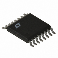
LT1765EFE-3.3 Linear Technology, LT1765EFE-3.3 Datasheet - Page 12

LT1765EFE-3.3
Manufacturer Part Number
LT1765EFE-3.3
Description
IC REG SW STEPDOWN 3A 16-TSSOP
Manufacturer
Linear Technology
Type
Step-Down (Buck)r
Datasheet
1.LT1765ES8PBF.pdf
(20 pages)
Specifications of LT1765EFE-3.3
Internal Switch(s)
Yes
Synchronous Rectifier
No
Number Of Outputs
1
Voltage - Output
3.3V
Current - Output
3A
Frequency - Switching
1.25MHz
Voltage - Input
3 ~ 25 V
Operating Temperature
-40°C ~ 125°C
Mounting Type
Surface Mount
Package / Case
16-TSSOP Exposed Pad, 16-eTSSOP, 16-HTSSOP
Lead Free Status / RoHS Status
Contains lead / RoHS non-compliant
Power - Output
-
Available stocks
Company
Part Number
Manufacturer
Quantity
Price
Part Number:
LT1765EFE-3.3
Manufacturer:
LINEAR/凌特
Quantity:
20 000
Company:
Part Number:
LT1765EFE-3.3#PBF
Manufacturer:
LT
Quantity:
7 000
Company:
Part Number:
LT1765EFE-3.3#TRPBF
Manufacturer:
LT
Quantity:
7 000
Part Number:
LT1765EFE-3.3#TRPBF
Manufacturer:
LINEAR/凌特
Quantity:
20 000
APPLICATIONS INFORMATION
APPLICATIONS INFORMATION
LT1765/LT1765-1.8/LT1765-2.5/
LT1765-3.3/LT1765-5
rating. A ground plane should always be used under the
switcher circuitry to prevent interplane coupling and
overall noise.
The V
possible from the switch and boost nodes. The LT1765
pinout has been designed to aid in this. The ground for
these components should be separated from the switch
current path. Failure to do so will result in poor stability
or subharmonic like oscillation.
Board layout also has a signifi cant effect on thermal
resistance. The exposed pad or GND pin is a continuous
copper plate that runs under the LT1765 die. This is the
best thermal path for heat out of the package as can be
seen by the low θ
ing the thermal resistance from Pin 4 or exposed pad
onto the board will reduce die temperature and increase
the power capability of the LT1765. This is achieved by
providing as much copper area as possible around this
pin/pad. Also, having multiple solder fi lled feedthroughs
to a continuous copper plane under LT1765 will help in
reducing thermal resistance. Ground plane is usually suit-
able for this purpose. In multilayer PCB designs, placing a
ground plane next to the layer with the LT1765 will reduce
thermal resistance to a minimum.
12
INPUT
CERAMIC
15V
4.7μF
C3
C
OFF
and FB components should be kept as far away as
ON
V
SHDN
SYNC
IN
JC
LT1765-33
of the exposed pad package. Reduc-
BOOST
GND
V
C
V
0.18μF
SW
FB
C
2.2nF
C
C2
Figure 6. Typical Application and Layout (Topside Only Shown)
D1
B220A
CMDSH-3
2.7μH
L1
D2
1765 F06
C1
4.7μF
CERAMIC
OUTPUT
3.3V
2.5A
KELVIN
SENSE
THERMAL CALCULATIONS
Power dissipation in the LT1765 chip comes from four
sources: switch DC loss, switch AC loss, boost circuit cur-
rent, and input quiescent current. The following formulas
show how to calculate each of these losses. These formulas
assume continuous mode operation, so they should not
be used for calculating effi ciency at light load currents.
Switch loss:
Boost current loss for VBOOST = VOUT:
Quiescent current loss:
R
17ns = Equivalent switch current/voltage overlap time
f = Switch frequency
V
SW
OUT
P
P
P
SW
Q
BOOST
= Switch resistance (≈0.13Ω at hot)
V OUT
V IN
=
L1
D2
C2
=
V
IN
R
=
(
SW OUT
0 001
C1
V
.
OUT
MINIMIZE D1, C3
(
I
LT1765 LOOP
D1
)
V
2
IN
(
) (
V
I
2
OUT
IN
GND
C3
V
OUT
/
50
)
)
+
17
GND
ns I
1765 F6a
C
(
C
OUT
KEEP FB AND V
COMPONENTS AND
TRACES AWAY FROM
HIGH FREQUENCY,
HIGH INPUT
COMPONENTS
PLACE FEEDTHROUGHS
UNDER AND AROUND
GROUND PAD FOR
GOOD THERMAL
CONDUCTIVITY
)( )( )
V
IN
f
C
1765fd


