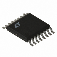
LT3434EFE#TRPBF Linear Technology, LT3434EFE#TRPBF Datasheet - Page 19

LT3434EFE#TRPBF
Manufacturer Part Number
LT3434EFE#TRPBF
Description
IC REG SW BUCK 3A 200KHZ 16TSSOP
Manufacturer
Linear Technology
Type
Step-Down (Buck)r
Datasheet
1.LT3434EFEPBF.pdf
(24 pages)
Specifications of LT3434EFE#TRPBF
Internal Switch(s)
Yes
Synchronous Rectifier
No
Number Of Outputs
1
Voltage - Output
1.25 ~ 54 V
Current - Output
3A
Frequency - Switching
200kHz
Voltage - Input
3.3 ~ 60 V
Operating Temperature
-40°C ~ 125°C
Mounting Type
Surface Mount
Package / Case
16-TSSOP Exposed Pad, 16-eTSSOP, 16-HTSSOP
Lead Free Status / RoHS Status
Lead free / RoHS Compliant
Power - Output
-
Available stocks
Company
Part Number
Manufacturer
Quantity
Price
threshold during normal operation, the C
discharged and PG inactive, resulting in a non Power Good
cycle when SHDN is taken above its threshold. Figure 9
shows the power good operation with PGFB connected to
FB and the capacitance on C
a limited amount of driver capability and is susceptible to
APPLICATIO S I FOR ATIO
100k TO V
500mV/DIV
500mV/DIV
2V/DIV
V
V
SHDN
OUT
V
PG
CT
IN
PG at 80% V
V
OUT
Figure 9. Power Good
LT3434
LT3434
U
PGFB
PGFB
Disconnect at 80% V
V
with 100ms Delay
V
PG
PG
TIME (10ms/DIV)
FB
C
FB
C
IN
IN
T
T
U
OUT
T
= 0.1µF. The PGFB pin has
with 100ms Delay
0.27µF
0.27µF
200k
W
200k
153k
12k
100k
153k
12k
100k
OUT
3434 F09
T
C
C
Figure 10. Power Good Circuits
pin will be
OUT
OUT
V
U
OUT
= 3.3V
V
OUT
= 3.3V
V
noise during start-up and Burst Mode operation. If erratic
operation occurs during these conditions a small filter
capacitor from the PGFB pin to ground will ensure proper
operation. Figure 10 shows several different configura-
tions for the LT3434 Power Good circuitry.
LAYOUT CONSIDERATIONS
As with all high frequency switchers, when considering
layout, care must be taken in order to achieve optimal
electrical, thermal and noise performance. For maximum
efficiency switch rise and fall times are typically in the
nanosecond range. To prevent noise both radiated and
conducted the high speed switching current path, shown
in Figure 11, must be kept as short as possible. This is
implemented in the suggested layout of Figure 12. Short-
ening this path will also reduce the parasitic trace induc-
tance of approximately 25nH/inch. At switch off, this
parasitic inductance produces a flyback spike across the
OUT
PG at V
LT3434
LT3434
Disconnect 3.3V Logic Signal
PGFB
PGFB
IN
with 100µs Delay
V
V
PG
PG
FB
C
FB
C
IN
IN
> 4V with 100ms Delay
T
T
511k
200k
0.27µF
270pF
200k
200k
165k
100k
866k
100k
3434 F10
C
OUT
C
V
OUT
OUT
= 3.3V
V
OUT
= 12V
LT3434
19
3434fb


