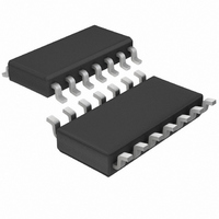
LTC1148HVIS-5#TRPBF Linear Technology, LTC1148HVIS-5#TRPBF Datasheet - Page 13

LTC1148HVIS-5#TRPBF
Manufacturer Part Number
LTC1148HVIS-5#TRPBF
Description
IC SW REG STEP-DOWN 5V 14-SOIC
Manufacturer
Linear Technology
Type
Step-Down (Buck)r
Datasheet
1.LTC1148CSPBF.pdf
(20 pages)
Specifications of LTC1148HVIS-5#TRPBF
Internal Switch(s)
No
Synchronous Rectifier
Yes
Number Of Outputs
1
Voltage - Output
5V
Current - Output
50mA
Frequency - Switching
250kHz
Voltage - Input
3.5 ~ 20 V
Operating Temperature
-40°C ~ 85°C
Mounting Type
Surface Mount
Package / Case
14-SOIC (3.9mm Width), 14-SOL
Lead Free Status / RoHS Status
Lead free / RoHS Compliant
Power - Output
-
APPLICATIO S I FOR ATIO
and δ
for each MOSFET can now be calculated:
The P-channel requirement can be met by a Si9430DY,
while the N-channel requirement is exceeded by a
Si9410DY. Note that the most stringent requirement for
the N-channel MOSFET is with V
During a continuous short circuit, the worst-case
N-channel dissipation rises to:
With the 0.05Ω sense resistor I
increasing the 0.085Ω N-channel dissipation to 450mW at
a die temperature of 73°C.
C
temperature, and C
optimum efficiency.
Now allow V
voltages the operating frequency will decrease and the
P-channel will be conducting most of the time, causing its
power dissipation to increase. At V
This last step is necessary to assure that the power
dissipation and junction temperature of the P-channel are
not exceeded.
LTC1148 Adjustable Applications
When an output voltage other than 3.3V or 5V is required,
the LTC1148 adjustable version is used with an external
resistive divider from V
regulated voltage is determined by:
IN
P
P-Ch R
N-Ch R
P
V
f
MIN
N
will require an RMS current rating of at least 1A at
P
OUT
P
= I
=
= δ
= (1/2.92µs)[1 – (5V/7V)] = 98kHz
SC(AVG)
= 1.25
5V(0.12Ω)(2A)
N
DS(ON)
DS(ON)
= 0.007(63 – 25) = 0.27. The required R
IN
to drop to its minimum value. At lower input
2
)
(R
1 + R2
=
=
DS(ON)
OUT
7V
U U
5(2)
7(2)
R1
12(0.25)
12(0.25)
OUT
will require an ESR of 0.05Ω for
2
2
)
2
)(1 + δ
(1.27)
(1.27)
(1.27)
to V
FB
OUT
N
SC(AVG)
Pin 9 (see Figure 9). The
= 0.12Ω
= 0.085Ω
)
= 435mW
IN(MIN)
= 0 (i.e., short circuit).
W
= 2A will result,
= 7V:
U
DS(ON)
To prevent stray pickup a 100pF capacitor is suggested
across R1 located close to the LTC1148.
For Figure 1 applications with V
R
inputs operate near ground. When the current comparator
is operated at less than 2V common mode, the off time
increases approximately 40%, requiring the use of a
smaller timing capacitor C
Auxiliary Windings – Suppressing Burst Mode
Operation
The LTC1148 synchronous switch removes the normal
limitation that power must be drawn from the inductor
primary winding in order to extract power from auxil-
iary windings. With synchronous switching, auxiliary
outputs may be loaded without regard to the primary
output load, providing that the loop remains in continu-
ous mode operation.
Burst Mode operation can be suppressed at low output
currents with a simple external network which cancels the
25mV minimum current comparator threshold. This tech-
nique is also useful for eliminating audible noise from
certain types of inductors in high current (I
applications when they are lightly loaded.
An external offset is put in series with the SENSE
subtract from the built-in 25mV offset. An example of this
technique is shown in Figure 6. Two 100Ω resistors are
inserted in series with the leads from the sense resistor.
SENSE
SENSE
SENSE
is moved to ground, the current sense comparator
Figure 6. Suppression of Burst Mode Operation
+
–
(PIN 8)
(PIN 7)
LTC1148-3.3/LTC1148-5
R3
1000pF
T
.
100Ω
100Ω
R2
R1
OUT
below 2V, or when
LTC1148
+
R
OUT
LTC1148 • F06
SENSE
C
OUT
V
13
–
OUT
> 5A)
pin to
114835fd


